
PUBLISHER: Information Network | PRODUCT CODE: 1478710

PUBLISHER: Information Network | PRODUCT CODE: 1478710
Flip Chip/WLP Manufacturing and Market Analysis
Introduction
The semiconductor industry is continually evolving, driven by advancements in packaging technologies that enhance performance, reliability, and miniaturization of electronic devices. Among these technologies, Flip Chip and Wafer-Level Packaging (WLP) have emerged as critical enablers of next-generation semiconductor devices. These packaging techniques offer unparalleled advantages in terms of size reduction, increased functionality, and improved electrical performance, making them indispensable in modern electronic systems.
The semiconductor Flip Chip and WLP market have witnessed significant growth in recent years, fueled by the growing demand for compact, high-performance electronic devices across various end-use industries such as consumer electronics, automotive, healthcare, and telecommunications. As manufacturers strive to meet the ever-increasing demands for smaller form factors, higher functionality, and greater reliability, Flip Chip and WLP technologies have become essential solutions for addressing these challenges.
This comprehensive report on semiconductor Flip Chip and WLP provides a detailed analysis of the market landscape, including key trends, drivers, challenges, and opportunities shaping the industry's trajectory. With a focus on technological advancements, market dynamics, and competitive landscape, this report aims to provide stakeholders with valuable insights to make informed decisions and capitalize on emerging market trends.
Key components of the report include:
Market Overview: An in-depth overview of the semiconductor Flip Chip and WLP market, including market size, growth drivers, and industry challenges. The report examines the current market landscape and provides forecasts for market growth and adoption trends over the forecast period.
Technology Landscape: A comprehensive analysis of Flip Chip and WLP technologies, including their principles, manufacturing processes, and key advancements. The report explores emerging trends such as fan-out wafer-level packaging (FOWLP), through-silicon vias (TSVs), and heterogeneous integration, highlighting their impact on the semiconductor packaging ecosystem.
Application Insights: An examination of key application areas driving the adoption of Flip Chip and WLP technologies across various industries, including consumer electronics, automotive electronics, healthcare devices, and telecommunications infrastructure. The report identifies growth opportunities and market trends in each application segment.
Competitive Analysis: A detailed assessment of the competitive landscape, including the profiles of leading players, their product portfolios, key strategies, and recent developments. The report provides insights into market positioning, competitive strengths, and potential growth strategies adopted by key players in the semiconductor Flip Chip and WLP market. Market Outlook and Opportunities: A forward-looking analysis of market trends, emerging opportunities, and future growth prospects in the semiconductor Flip Chip and WLP market. The report offers strategic recommendations for stakeholders to capitalize on market opportunities and mitigate potential risks.
Trends in Semiconductor Flip Chip/WLP (Wafer Level Packaging)
In the fast-paced world of semiconductor manufacturing, innovation drives progress. Among the myriad of advancements, Flip Chip and Wafer-Level Packaging (WLP) have emerged as pivotal technologies revolutionizing the landscape of electronic devices. With a focus on size reduction, enhanced performance, and increased functionality, these packaging techniques are reshaping the way semiconductor components are integrated, paving the way for a new era of compact, high-performance electronics. In this article, we delve into the latest trends shaping the semiconductor Flip Chip/WLP market, exploring the key drivers, innovations, and opportunities propelling this dynamic industry forward.
Market Growth and Expansion:
The semiconductor Flip Chip/WLP market is experiencing robust growth, driven by the escalating demand for smaller, more powerful electronic devices across a multitude of industries. With advancements in manufacturing processes and material technologies, Flip Chip and WLP solutions are increasingly being adopted in applications ranging from smartphones and wearables to automotive electronics and IoT devices. The market is poised for further expansion as manufacturers seek innovative packaging solutions to meet the evolving needs of modern electronic systems.
Technological Advancements:
Technological innovation lies at the heart of Flip Chip and WLP advancements. One of the key trends shaping the market is the adoption of fan-out wafer-level packaging (FOWLP), which offers significant advantages in terms of cost efficiency, miniaturization, and improved electrical performance. Additionally, through-silicon vias (TSVs) have emerged as a critical enabler of 3D integration, allowing for greater integration density and enhanced performance in semiconductor devices. Other notable trends include the development of heterogeneous integration techniques and the integration of advanced materials such as silicon photonics and gallium nitride (GaN) into packaging processes.
Application Diversification:
Flip Chip and WLP technologies are finding applications across a diverse range of industries, driving demand for specialized packaging solutions tailored to specific end-use requirements. In the consumer electronics sector, Flip Chip/WLP solutions are facilitating the development of smaller, more energy-efficient devices with enhanced functionality. In the automotive industry, these technologies are enabling the integration of advanced driver-assistance systems (ADAS), infotainment systems, and vehicle-to-everything (V2X) communication modules. Moreover, in the healthcare and telecommunications sectors, Flip Chip/WLP solutions are playing a crucial role in the development of next-generation medical devices, network infrastructure, and 5Genabled devices.
Market Dynamics and Competitive Landscape:
The semiconductor Flip Chip/WLP market is characterized by intense competition and rapid technological advancements. Leading players in the industry are investing heavily in research and development to stay ahead of the curve and gain a competitive edge. Moreover, strategic partnerships, mergers, and acquisitions are shaping the competitive landscape, driving consolidation and fostering innovation. As the market continues to evolve, collaboration between semiconductor manufacturers, packaging companies, and equipment suppliers will be crucial to unlocking new opportunities and driving growth.
Future Outlook and Opportunities:
Looking ahead, the future of the semiconductor Flip Chip/WLP market looks promising, with ample opportunities for innovation and growth. Continued advancements in packaging technologies, coupled with the proliferation of emerging applications such as artificial intelligence (AI), Internet of Things (IoT), and automotive electronics, are expected to drive demand for Flip Chip and WLP solutions. Moreover, as semiconductor devices become increasingly complex and heterogeneous, the need for advanced packaging solutions will only continue to grow, presenting new opportunities for market players to capitalize on.
Table of Contents
Chapter 1. Introduction
Chapter 2. Executive Summary
Chapter 3. Flip Chip/WLP Issues and Trends
- 3.1. Introduction
- 3.2. Wafer Bumping
- 3.2.1. Solder Bumps
- 3.2.1.1. Metallurgy
- 3.2.1.2. Deposition Of UBM
- 3.2.1.3. Sputter Etching
- 3.2.1.4. Photolithography
- 3.2.1.5. Solder Deposition
- 3.2.1.6. Resist Strip
- 3.2.1.7. UBM Wet Etch
- 3.2.1.8. Reflow
- 3.2.1.9. Flux Issues
- 3.2.2. Gold Bumps
- 3.2.2.1. Bump Processing
- 3.2.2.2. Bonding
- 3.2.2.3. Coplanarity
- 3.2.2.4. Conductivity
- 3.2.2.5. Thermal Properties
- 3.2.2.6. Size
- 3.2.2.7. Reliability
- 3.2.2.8. Cost Issues
- 3.2.3. Copper Pillar Bumps
- 3.2.4. Copper Stud Bumping
- 3.2.5. C4NP
- 3.2.1. Solder Bumps
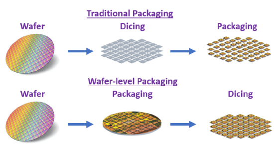
- 3.3. Wafer Level Packaging
- 3.4. Pad Redistribution
- 3.5. Wafer Bumping Costs
- 3.5.1. Wafer Redistribution And Wafer Bumping Costs
- 3.5.2. WLCSP Hidden Costs
- 3.5.3. WLCSP Cost Per Good Die
- 3.5.4. Wafer-Level Underfill Costs
- 3.6. Panel Level Packaging
Chapter 4. Lithography Issues And Trends
- 4.1. Issues
- 4.1.1. Technical Performance
- 4.1.2. Capital Investment
- 4.1.3. Cost Of Consumables
- 4.1.4. Throughput
- 4.1.5. Ease Of Use
- 4.1.6. Flexibility
- 4.1.7. Equipment Support
- 4.1.8. Resolution
- 4.1.9. Solder Bumping Capabilities
- 4.1.10. Gold Bumping Capabilities
- 4.2. Exposure Systems
- 4.2.1. Introduction
- 4.2.1.1. Reduction Steppers 4.
- 4.2.1.2. Full-Field Projection
- 4.2.1.3. Mask Aligners
- 4.2.1.4. 1X Steppers
- 4.2.1.5. 2X Steppers
- 4.2.1. Introduction
- 4.3. Competitive Technologies
- 4.3.1. Inkjet Printing
- 4.3.2. Stencil/Screen Printing
- 4.3.3. Electroless Metal Deposition
Chapter 5. UBM Etch Issues And Trends
- 5.1. Introduction
- 5.2. Technology Issues And Trends
- 5.2.1. Process Flow
- 5.2.2. Etch Process
- 5.2.3. Etch Chemistry
- 5.3. Batch Versus Single-Wafer Etching
Chapter 6. Metallization Issues and Trends
- 6.1. Introduction
- 6.2. Sputtering Metallization
- 6.2.1. Gold Bump
- 6.2.2. Solder Bumping
- 6.2.2.1. T I / Cu and TiW / Cu
- 6.2.2.2. Al / NiV / Cu
- 6.2.2.3. T i / N i (V) and TiW / Ni ( V )
- 6.2.2.4. Cr / Cr-Cu / Cu
- 6.2.3. Copper Bumping
- 6.3. Electrodeposition
Chapter 7. Market Analysis
- 7.1. Market Drivers For Flip Chip And WLP
- 7.2. Market Opportunities
- 7.3. Challenges
- 7.4. Flip Chip Market
- 7.4.1. Market Dynamics
- 7.4.2. Market Forecast
- 7.5. Lithography Market
- 7.5.1. Aligners Vs. Steppers
- 7.5.2. Market Analysis
- 7.6. Deposition Market
List of Tables
- 3.1. Common UBM Stacks For Solder And Gold Bumping
- 3.2. Solder Bumping Guidelines
- 3.3. Gold Bumping Guidelines
- 3.4. Copper Bumping Guidelines
- 3.5. Comparison Of Solder Bumping Processes
- 3.6. ITRS Pin Counts For Different Applications
- 3.7. Pillar-WLP CSP Guidelines
- 3.8. Pad Redistribution Guidelines
- 4.1. Key Challenges For WLP Lithography
- 4.2. Lithography Tools By Vendor
- 5.1. UBM Film Etchants
- 5.2. Advantages Of Spin Processing
- 6.1. Common UBM Stacks For Gold And Solder Bumping
- 7.1. WLP Demand by Device (Units)
- 7.2. WLP Demand by Device (Wafers)
- 7.3. Worldwide Lithography Forecast
- 7.4. Cost Of Ownership Of 1x Versus 2x Steppers
- 7.5. Worldwide Forecast For Deposition Tools
List of Figures
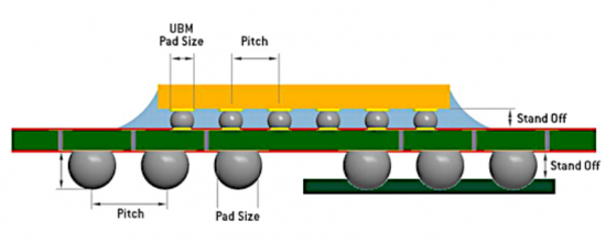
- 3.1. C4 Chip Connections
- 3.2. Wafer Bump Technology Roadmap
- 3.3. Comparison Of Copper Pillar, Flip Chip, And WLP
- 3.4. Solder Bumping Process
- 3.5. Three Process Flows For Solder Bumping
- 3.6. Gold Bumping Process
- 3.7. Cost Per Gold Bumped Wafer
- 3.8. Copper Stud Bump
- 3.9. Breakdown Of Stud Bumping Costs
- 3.10. C4NP Process Description
- 3.11. Pillar-WLPCSP Process
- 3.12. Pad Redistribution Process
- 4.1. Laser-Projection Imaging
- 4.2. Solder Jet Technology
- 4.3. Principle Of Screen Printing
- 4.4. Principle Of Inkjet Printing
- 4.5. Electroless Under Bump Metallization
- 5.1. Electroplated Solder Bumping Process
- 7.1. WLP Applications
- 7.2. Wire Bond versus Flip Chip
- 7.3. Flip Chip and Wire Bond Equipment Forecast
- 7.4. Growth in Copper Wire Bonding
- 7.5. Flip Chip Market By Number of Devices
- 7.6. Flip Chip Market By Number of Wafers
- 7.7. WLP Market by Device - 2014
- 7.8. WLP Market by Device - 2020
- 7.9. Device Shipment Forecast WLP Vs Flip Chip
- 7.10. Device Shipment Forecast FIWLP Vs FOWLP
- 7.11. Historic Lithography Market Shares
- 7.12. Lithography Market Share Growth
- 7.13. ECD Market Shares
- 7-14. Sputtering Market Shares

