
PUBLISHER: Mordor Intelligence | PRODUCT CODE: 1433831

PUBLISHER: Mordor Intelligence | PRODUCT CODE: 1433831
Gallium Arsenide GaAs Wafer - Market Share Analysis, Industry Trends & Statistics, Growth Forecasts (2024 - 2029)
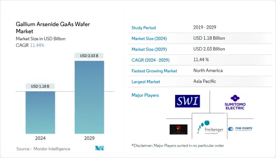
The Gallium Arsenide GaAs Wafer Market size is estimated at USD 1.18 billion in 2024, and is expected to reach USD 2.03 billion by 2029, growing at a CAGR of 11.44% during the forecast period (2024-2029).
GaAs is mainly used is common in electronics, such as semiconductor manufacturing. The growing adoption of GaAs wafers in products such as LEDs, laser diodes, optoelectronic devices, and monolithic microwave integrated circuits is considered among the primary factors driving the growth of the studied market. The price of this compound being regulated creates more growth opportunities for gallium arsenide (GaAs) wafers manufacturers.
Gallium Arsenide or GaAs is a compound material made up of two elements. The semiconductor used to manufacture GaAs wafers is a direct bandgap semiconductor, meaning that electrons can pass through components much quicker without much interference, making them particularly useful in optoelectronic devices.
The increasing adoption of smartphones and computing devices and the growing penetration of light-emitting diodes (LEDs) in general lighting are significant growth drivers for this market. The advent of IoT has also been one of the major reasons responsible for the increasing market trend. The technology has also created a demand for high-frequency communication devices with GaAs-based ICs.
As a result, with several telecommunication companies expanding their communication infrastructure, the demand for GaAs wafers will increase, which will positively influence the growth of the studied market in the forthcoming years. Additionally, owing to its inherent features, the need for GaAs wafers across various end-user industries such as electronics, aerospace & defense, and communications is increasing, which, in turn, is also driving the demand for GaAs Wafers globally.
For instance, GaAs wafers are also a great choice for high-power outer space electronics and optical windows due to their wide direct bandgap material that resists radiation damage which is also predicted to offer profitable chances for market expansion and give rise to new market trends and use cases, including their higher adoption in electronic warfare systems, electric aircraft, and developments in broadband cellular network technology.
However, the price of GaAs wafers is among the major disadvantage, which explains its low utilization. To solve such issues, researchers have achieved new methods of manufacturing thin films of low-cost gallium arsenide to help create devices that would replace silicon to support the studied market's growth.
The global outbreak of the COVID-19 pandemic and the subsequent decisive government actions taken to curb the spread of the virus had a notable impact on the semiconductor sector, affecting the manufacture of semiconductor components and lowering customer demand, thereby impeding the global market's growth. However, higher exposure to digital technologies significantly enhanced the demand for advanced consumer electronic devices and supporting digital infrastructure, which positively influenced the growth of the studied market.
Gallium Arsenide (GaAs) Wafer Market Trends
Radio Frequency Electronics to Hold the Significant Share in the Market
Radio-frequency (RF) devices produced with GaAs substrates are widely used in wireless communication applications, including wireless networks (WLAN), 4G/5G base stations, mobile communication, satellite, and Wi-Fi communications. The development of such trends marks an important milestone in developing next-generation, ultra-compact, and high-performance RF front-end chipsets that are needed for smartphones and other handsets, supporting 4G and 5G services.
GaAs wafers' higher efficiency and lower power consumption are also enticing market participants to adopt them, positively influencing the demand for GaAs wafers. Optoelectronic devices were previously widely used in computer peripherals and short-range optical communications. Still, they are in high order for new applications such as augmented reality (AR), lidar, and facial recognition.
Globally, internet penetration is rising, especially in developing countries such as India and Brazil, stimulating the demand for GaAs wafers. Subsequently, the need for fiber-optic networks and backhaul, base stations, and Wi-Fi connectivity products with wireless communication infrastructure and have supported the growing penetration of the internet worldwide, which, in turn, is driving the adoption of GaAs wafers.
Further, the growth of mobile data consumption rate and the wide adoption of IoT devices also propel the requirement for Wi-Fi and other wireless communication devices. As a result of the high growth rates for such products and technologies related to wireless communications are aiding the adoption of GaAs wafers. For instance, according to 5G America, the global number of mobile 5G subscriptions is expected to grow from 1.9 million in 2023 to 5.9 million by 2027.
Asia Pacific to Dominate the Market During the Forecast Period
The Asia Pacific region has an increasing demand for intelligent consumer electronic devices. China, Taiwan, Japan, and India have surging demand for advanced technological devices such as smartphones, wearables, computers, and laptops, further augmenting the regional market's growth. GaAs products offer better connectivity through enhanced data transmission and quality than silicon-based devices, so their demand has increased. Additionally, GaAs products can be manufactured on large scales with high yield rates, which improves business growth. The increasing Internet penetration, expansion of 4G and 5G networks, and the electronic industry are also expected to fuel the development of the GaAs wafer market in the region.
One major driving factor in the Asia Pacific region is the growing demand for advanced technological devices such as computing devices, smartphones, tablets, and laptops. As GaAs products such as transistors can be used for smartphones and other wireless communication devices, the growing demand is driving the need for GaAs wafers at a promising rate.
China is the major country dominating the market for the electronics industry owing to considerable government support, which is fostering the development of the studied market in China. For instance, the Chinese government is promoting its domestic technology market by funding the industry players. Such trends are encouraging new players to expand their presence in the country. For instance, in February 2023, AXT, a manufacturer of compound semiconductor wafer substrates such as GaAs wafer substrates, announced an expansion of operations at its Beijing facility. The company invested in raw material extraction facilities to further strengthen its position as the leading provider of compound semiconductor substrates.
China is also among the leading countries in 5G infrastructure development and adopting other consumer electronic and electric mobility solutions. For instance, according to MIIT, by the end of 2022, China had about 2.31 million 5G base stations. Together the growth of these industries is creating a favorable outlook for the growth of the studied market in China.
Taiwan has witnessed the wafer market as one of the critical areas of technological development. As a result, Taiwan is also expected to hold a significant market share in the global GaAs wafer market. Companies across Taiwan are addressing the supply chain needs of front and back-end advanced wafer-level packaging architectures to cater to specialty materials and processes, thus, influencing the overall market studied.
Gallium Arsenide (GaAs) Wafer Industry Overview
The Gallium Arsenide GaAs Wafer Market is competitive and highly concentrated with a few companies such as AXT Inc, Sumitomo Electric Industries Ltd., Semiconductor Wafer Inc, Freiberger Compound Materials GmbH, Xiamen Powerway Advanced Material Co. Ltd, holding a significant market share. Established companies focus on strengthening their position by investing heavily in R&D and providing customers with better and technologically advanced products.
In May 2023, QE, a semiconductor wafer specialist, introduced a new range of 200mm RGB epitaxial wafer products specifically designed for microLED display qualification. According to the company, GaN and GaAs epitaxy is anticipated to continue to play a crucial role in driving the rapid adoption of microLEDs.
In May 2022, The MOSIS Service of Information Sciences Institute, University of Southern California, and WIN Semiconductors Corp. signed a Memorandum of Understanding (MoU) to accelerate the development of GaAs and GaN monolithic microwave integrated circuits with WIN Semiconductors' GaAs and GaN process technologies. The partnership will support the reliable, innovative, and effective design and prototyping flow through the multi-project wafer (MPW) projects with the MOSIS Service and WIN Semiconductors.
Additional Benefits:
- The market estimate (ME) sheet in Excel format
- 3 months of analyst support
TABLE OF CONTENTS
1 INTRODUCTION
- 1.1 Study Assumptions and Market Definition
- 1.2 Scope of the Study
2 RESEARCH METHODOLOGY
3 EXECUTIVE SUMMARY
4 MARKET INSIGHTS
- 4.1 Market Overview
- 4.2 Industry Attractiveness - Porter's Five Forces Analysis
- 4.2.1 Bargaining Power of Suppliers
- 4.2.2 Bargaining Power of Buyers
- 4.2.3 Threat of New Entrants
- 4.2.4 Threat of Substitute Products
- 4.2.5 Intensity of Competitive Rivalry
- 4.3 Technology Snapshot
- 4.3.1 Liquid Encapsulated Czochralski (LEC) Grown GaAs
- 4.3.2 Vertical Gradient Freeze (VGF) Grown GaAs
- 4.4 Assessment of the Impact of COVID-19 on the Market
5 MARKET DYNAMICS
- 5.1 Market Drivers
- 5.1.1 Increasing Adoption of 5G Infrastructure Across the World
- 5.1.2 Surging Demand for Opto-electronic Devices
- 5.2 Market Restraints
- 5.2.1 High Production Cost
6 MARKET SEGMENTATION
- 6.1 By Application
- 6.1.1 Radio Frequency Electronics
- 6.1.2 Light Emitting Diodes
- 6.1.3 Photovoltaic Devices
- 6.1.4 Phototonic Devices
- 6.1.5 Other Applications
- 6.2 By Geography
- 6.2.1 United States
- 6.2.2 Taiwan
- 6.2.3 China
- 6.2.4 Japan
- 6.2.5 United Kingdom
- 6.2.6 Germany
- 6.2.7 Rest of the World
7 COMPETITIVE LANDSCAPE
- 7.1 Company Profiles
- 7.1.1 Semiconductor Wafer Inc
- 7.1.2 AXT Inc.
- 7.1.3 Freiberger Compound Materials GmbH
- 7.1.4 Xiamen Powerway Advanced Material Co. Ltd.
- 7.1.5 Sumitomo Electric Industries Ltd.
- 7.1.6 Wafer Technology Ltd.
- 7.1.7 MTI Corporation
- 7.1.8 Vital Materials Co Limited
- 7.1.9 Dowa Electronics Materials Co. Ltd.
- 7.1.10 American Elements
8 INVESTMENT ANALYSIS
9 MARKET OPPORTUNITIES AND FUTURE TRENDS

