
PUBLISHER: Mordor Intelligence | PRODUCT CODE: 2043877

PUBLISHER: Mordor Intelligence | PRODUCT CODE: 2043877
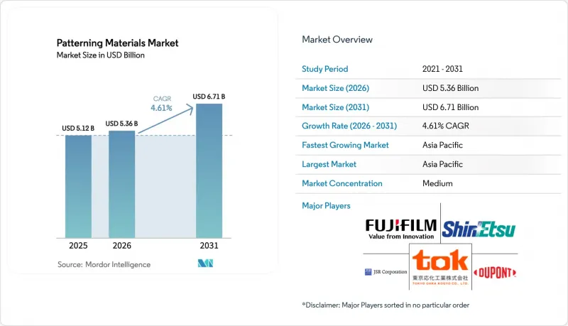
Patterning Materials - Market Share Analysis, Industry Trends & Statistics, Growth Forecasts (2026 - 2031)
The Patterning Materials Market size is expected to grow from USD 5.12 billion in 2025 to USD 5.36 billion in 2026 and is forecast to reach USD 6.71 billion by 2031 at 4.61% CAGR over 2026-2031.
At the sub-3 nm nodes, premium extreme-ultraviolet (EUV) and high-numerical-aperture (high-NA) photoresists are capturing significant value. In contrast, legacy 193 nm dry and immersion chemistries continue to dominate, serving as the high-volume workhorses for mature nodes. These mature nodes primarily cater to sectors such as automotive, industrial, and the Internet of Things. The Asia-Pacific region, bolstered by subsidy-driven expansions in Japan and the establishment of new fabs in China, now accounts for a significant portion of global wafer starts. This dominance ensures a consistent demand for mainstream resists and premium anti-reflective coatings. Geopolitical tensions are reshaping the landscape of patterning materials. Notably, Japan's state-backed acquisition of JSR and its export restrictions have heightened dependency concerns for international buyers. On another front, trends such as automotive electrification, the adoption of back-side power delivery, and the emergence of chiplet packaging are not only modifying resist film thickness requirements but also broadening revenue prospects for specialty formulations. This shift is helping to mitigate unit-price declines in the mature-node segment.
Global Patterning Materials Market Trends and Insights
Rapid Semiconductor Fab Expansion in Asia-Pacific
Between 2026 and 2029, dozens of subsidy-backed fabs, currently under construction in China, Japan, and South Korea, are poised to ramp up monthly production by millions of 300 mm wafer starts. This surge will heighten the structural demand for 193 nm dry, immersion, and top anti-reflective coatings, which are pivotal to the patterning materials market. TSMC has earmarked substantial capital for 2026, with a significant portion aimed at upgrading its Kumamoto campus to 3 nm lines. These advanced lines require both EUV and conventional resists in their multi-layer stacks. In a strategic initiative, Japan's Ministry of Economy, Trade and Industry has introduced incentives to strengthen local materials manufacturers. This move guarantees a consistent, short-haul supply of high-purity polymers and solvents. On the other hand, China is swiftly establishing 28 nm and 40 nm sites as a countermeasure to export controls. This strategy not only mitigates the impact of these controls but also ensures that positive 193 nm chemistries operate at peak capacity, even as EUV lithography gains traction. The implications of this strategy extend to thick-film resists, which are vital for advanced packaging redistribution layers. This is crucial since every newly designed logic die eventually integrates into a multichip module, demanding a finer RDL pitch.
EUV and High-NA Transition Driving Advanced Resist Demand
By early 2026, ASML's debut high-NA scanners showcased impressive uptime, efficiently processing a substantial number of wafers. This milestone highlights their commercial viability for nodes at 2 nm and below. The high-NA optics, which reduce the depth of focus by half, require a transition from chemically amplified resists to metal oxide and other high-absorption alternatives. This shift is essential to uphold pattern fidelity in films under 30 nm. ADEKA's Kashima line, slated to commence in 2028, will supply precursors to industry titans Samsung and SK Hynix. At the same time, Imec has successfully showcased 16 nm pitch capabilities, indicating readiness for mass production. This technology features a shortened exposure time, with metal atoms absorbing significantly more EUV photons. This enhancement not only reduces exposure duration but also lessens the stochastic defect rates typically seen with carbon-based polymers. However, due to capacity constraints, foundries are increasingly securing multi-year supply contracts. While these agreements raise immediate unit costs, they play a crucial role in safeguarding the essential high-NA ramp schedules.
High Cost and Limited Capacity of EUV-Grade Photoresists
Prices for EUV photoresist are several times higher than those for their 193 nm immersion counterparts. Additionally, EUV photoresists require specialized fluoride-free supply chains, which are rare among industry players. While only ADEKA and Inpria have publicly acknowledged their commercial-scale metal-oxide production, ADEKA's first production line is projected to reach its full capacity only by 2029. Currently, scanner shipments are limited, and orders for each high-NA tool heavily depend on a few long-term supply agreements. In light of this, foundries are overbooking their resist allocations, driving up costs per wafer during initial production ramps. This pricing pressure is underscored by Samsung's 2025 decision to reduce resist dispense per coat, revealing the revenue volatility in the patterning materials market.
Other drivers and restraints analyzed in the detailed report include:
- Automotive Electronics-Led Surge in Specialty Sensors
- Back-Side Power Delivery and GAA Devices Altering Resist Thickness Specs
- Stringent Solvent-Emission Regulations
For complete list of drivers and restraints, kindly check the Table Of Contents.
Segment Analysis
In 2025, the market for patterning materials saw a significant contribution from positive 193 nm dry resist, which commanded a 41.62% share. This segment is poised for steady growth, fueled by new Chinese fabs targeting 28 nm and 40 nm lines. On another front, top anti-reflective coatings are projected to grow at a rate of 6.54% during the forecast period of 2026-2031. This growth is largely attributed to the demands of EUV scanners, which require multilayer stacks to reduce reflective notching in high-NA optics. Brewer Science's anti-reflective technology has found a partner in Nissan Chemical. While positive 248 nm resists support legacy logic and thick-film MEMS, their growth is outpaced by the surging demand for newer chemistries. Metal oxide and vapor-deposited dry resists, while leading the pack, face significant uncertainties. Their future hinges on scalable deposition techniques and the regulatory green light for innovative photo-acid generators.
From 2026 to 2031, the competitive landscape is set to heat up. Incumbents in spin-coating are curbing dispense volumes to counter the threat of dry resist disruption. Meanwhile, endorsements from Lam Research and IBM for plasma-developed films, which promise advantages like triple photon absorption and single-print economics, are reshaping the patterning materials market. Once Europe establishes its thresholds, resists devoid of per- and polyfluoroalkyl substances might trigger a similar transformation for 248 nm and i-line materials. Suppliers proficient in both metal-oxide and fluorine-free polymers are poised to capture additional revenue streams by 2030.
The Patterning Materials Market Report is Segmented by Type (I-Line and G-Line, Positive 248 Nm, Positive 193 Nm Dry Resist, TARC, and Other Types), Application (Integrated Circuits and PCBs, MEMS and NEMS Devices, Sensors, Dynamic Random Access Memory, and Other Applications) and Geography (Asia-Pacific, North America, Europe, and Rest of the World). The Market Forecasts are Provided in Terms of Value (USD).
Geography Analysis
Asia-Pacific, accounting for 68.44% of global consumption in 2025, is projected to grow at a 6.83% CAGR through 2031. This growth is largely fueled by subsidy pools in Japan, China, and South Korea, bolstering their foundry and material ecosystems. In this region, JSR, Tokyo Ohka Kogyo, and Shin-Etsu Chemical dominate, leading the export of merchant photoresists. These companies strategically wield export licenses, enabling them to influence global wafer-start plans within weeks. While China's new fabs are set to outpace Taiwan in mature-node output by 2027, they still heavily depend on high-purity resist imports from Japan. This reliance makes China's national champions vulnerable to disruptions, especially given the current geopolitical climate.
North America, buoyed by the CHIPS Act, is witnessing a flurry of activity: Intel's mega-site in Ohio, TSMC's campus in Arizona, and Samsung's project in Taylor are all gearing up for substantial monthly wafer starts by 2030. DuPont is aggressively expanding, doubling its resist capacity at the Sasakami plant and debuting an advanced pilot line in Texas. Lam Research is making waves, introducing its Aether dry resist to U.S. logic producers. Despite facing approval backlogs for new photo-acid generators, multi-agency task forces, with defense funding backing, are hastening reviews, underscoring the region's commitment to the patterning materials market.
Europe, the smallest of the three core demand zones, is witnessing a surge in legislative activity. ESMC's Dresden fab, under the aegis of the EU Chips Act 2.0, is locally producing nodes for automotive applications. This has prompted Merck and BASF to boost their regional high-purity solvent output. However, ongoing discussions around PFAS cast a shadow on long-term prospects; a stringent threshold might necessitate a complete reformulation of every resist family. Suppliers are preemptively co-locating research and development in Japanese cleanrooms, where PFAS restrictions are more lenient. This move, while safeguarding their interests, inadvertently shifts intellectual property away from Europe, even as the wafer starts expanding within the continent.
- Allresist GmbH
- Applied Materials, Inc
- Brewer Science Inc.
- DONGJIN SEMICHEM CO., LTD
- DuPont
- Fujifilm Holdings Corporation
- Honeywell Electronic Materials, Inc
- JSR Corporation
- MacDermid, Inc
- Merck KGaA
- Microchem Corporation
- Nissan Chemical Corporation
- Samsung SDI
- Shin-Etsu Chemical Co., Ltd
- TOK TAIWAN CO., LTD.
- Tokyo Ohka Kogyo Co., Ltd
Additional Benefits:
- The market estimate (ME) sheet in Excel format
- 3 months of analyst support
TABLE OF CONTENTS
1 Introduction
- 1.1 Study Assumptions and Market Definition
- 1.2 Scope of the Study
2 Research Methodology
3 Executive Summary
4 Market Landscape
- 4.1 Market Drivers
- 4.1.1 Rapid semiconductor fab expansion in Asia-Pacific
- 4.1.2 EUV/High-NA transition driving advanced resist demand
- 4.1.3 Automotive electronics-led surge in specialty sensors
- 4.1.4 Back-side power delivery and GAA devices altering resist thickness specs
- 4.1.5 On-shoring incentives (US and EU Chips Acts) creating local supply pools
- 4.2 Market Restraints
- 4.2.1 High cost and limited capacity of EUV-grade photoresists
- 4.2.2 Stringent solvent-emission regulations
- 4.2.3 Metrology bottlenecks causing defect-related rework
- 4.3 Value Chain Analysis
- 4.4 Porter's Five Forces
- 4.4.1 Threat of New Entrants
- 4.4.2 Bargaining Power of Buyers
- 4.4.3 Bargaining Power of Suppliers
- 4.4.4 Threat of Substitutes
- 4.4.5 Degree of Competition
5 Market Size and Growth Forecasts (Value)
- 5.1 By Type
- 5.1.1 I-line and g-line
- 5.1.2 Positive 248 nm
- 5.1.3 Positive 193 nm Dry Resist
- 5.1.4 TARC
- 5.1.5 Other Types
- 5.2 By Application
- 5.2.1 Integrated Circuits and PCBs
- 5.2.2 MEMS and NEMS Devices
- 5.2.3 Sensors
- 5.2.4 Dynamic Random Access Memory
- 5.2.5 Other Applications
- 5.3 By Geography
- 5.3.1 Asia-Pacific
- 5.3.1.1 China
- 5.3.1.2 India
- 5.3.1.3 Japan
- 5.3.1.4 South Korea
- 5.3.1.5 ASEAN Countries
- 5.3.1.6 Rest of Asia-Pacific
- 5.3.2 North America
- 5.3.2.1 United States
- 5.3.2.2 Canada
- 5.3.2.3 Mexico
- 5.3.3 Europe
- 5.3.3.1 Germany
- 5.3.3.2 United Kingdom
- 5.3.3.3 France
- 5.3.3.4 Italy
- 5.3.3.5 Rest of Europe
- 5.3.4 Rest of the World
- 5.3.1 Asia-Pacific
6 Competitive Landscape
- 6.1 Market Concentration
- 6.2 Strategic Moves
- 6.3 Market Share(%)/Ranking Analysis
- 6.4 Company Profiles (includes Global Overview, Market Overview, Core Segments, Financials, Strategic Information, Products and Services, Recent Developments)
- 6.4.1 Allresist GmbH
- 6.4.2 Applied Materials, Inc
- 6.4.3 Brewer Science Inc.
- 6.4.4 DONGJIN SEMICHEM CO., LTD
- 6.4.5 DuPont
- 6.4.6 Fujifilm Holdings Corporation
- 6.4.7 Honeywell Electronic Materials, Inc
- 6.4.8 JSR Corporation
- 6.4.9 MacDermid, Inc
- 6.4.10 Merck KGaA
- 6.4.11 Microchem Corporation
- 6.4.12 Nissan Chemical Corporation
- 6.4.13 Samsung SDI
- 6.4.14 Shin-Etsu Chemical Co., Ltd
- 6.4.15 TOK TAIWAN CO., LTD.
- 6.4.16 Tokyo Ohka Kogyo Co., Ltd
7 Market Opportunities and Future Outlook
- 7.1 White-space and Unmet-Need Assessment

