
PUBLISHER: Mordor Intelligence | PRODUCT CODE: 2044004

PUBLISHER: Mordor Intelligence | PRODUCT CODE: 2044004
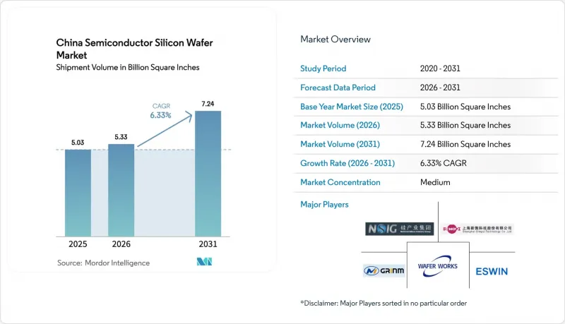
China Semiconductor Silicon Wafer - Market Share Analysis, Industry Trends & Statistics, Growth Forecasts (2026 - 2031)
The China Semiconductor Silicon Wafer Market size in terms of shipment volume is expected to grow from 5.03 Billion Square Inches in 2025 to 5.33 Billion Square Inches in 2026 and is forecast to reach 7.24 Billion Square Inches by 2031 at 6.33% CAGR over 2026-2031.
Robust government funding, tighter export controls on advanced foreign tools, and accelerating capacity additions by local foundries continue to propel demand. Beijing's 50%-domestic-equipment mandate, in force since early 2026, ties subsidies to the use of home-grown process tools, channeling incremental wafer orders toward Chinese suppliers. Rapid adoption of twelve-inch lines for logic and advanced analog devices, combined with rising electric-vehicle penetration, further elevates total substrate consumption. The market also benefits from surging chiplet-based AI accelerators that require ultra-flat prime wafers to enable hybrid bonding, even as lingering defect-density gaps versus Japanese incumbents keep high-end logic output partially import-dependent.
China Semiconductor Silicon Wafer Market Trends and Insights
Surge in 300 mm Capacity Build-Outs by Domestic Players
Semiconductor Manufacturing International Corporation confirmed late-2025 plans to add 40,000 twelve-inch wafer starts each month across Shanghai, Beijing, and Shenzhen fabs by end-2026, a move mirrored by Hua Hong Semiconductor's additional 20,000-wspm program targeting power-management ICs. Provincial incentives in land, taxes, and low-interest loans reduce upfront risk, allowing suppliers to sign multiyear take-or-pay contracts before capacity comes online. Shanghai Silicon Industry Group responded by scaling its Lingang plant to 2 million twelve-inch wafers a month for 2026 delivery. Scale economics below USD 50 per prime wafer become the tipping point, spurring a consolidation wave among smaller startups that cannot reach cost parity with these leaders.
Government "50% Domestic Tool" Mandate Accelerating Local Wafer Demand
Effective January 2026, the Ministry of Industry and Information Technology links subsidies to a minimum 50% local-tool adoption, ratcheting the threshold to 70% by 2028 and full localization in 2030. Foundries that fall short face subsidy claw-backs, so most streamline vendor lists to all-Chinese tool-and-wafer pairings. Naura Technology documented that over 60% of its deposition tools installed on 28 nm lines were matched with Shanghai Silicon substrates, trimming yield-ramp cycles by almost a quarter. Joint process-recipe sharing inside these closed loops accelerates progress on defect control and flattens the learning curve for new fabs.
Persistent Defect-Density Gap Vs. Japanese Suppliers in above 28 nm Logic Wafers
Average defect density of 0.12 defects cm-2 on domestic 300 mm prime wafers remains 50% above Shin-Etsu's 0.08 defects cm-2 benchmark, translating into roughly 8-10% lower yield for advanced mobile processors. Trace-metal contamination above 0.1 ppb in locally sourced polysilicon is a major contributor. Foundries compensate by implementing longer anneals and tighter incoming inspections, adding USD 15-20 per wafer in costs. High-volume fabless customers, therefore, stipulate Japanese substrates for leading-edge lots, capping the market ceiling for domestic suppliers despite capacity growth.
Other drivers and restraints analyzed in the detailed report include:
- Automotive SiC Power Device Boom Driving 200 mm and 8-Inch SiC Wafer Needs
- Rise of Advanced Packaging (Chiplet / X-DFOI) Lifting Demand for Ultra-Flat Prime Wafers
- U.S.-Led Export Controls Limiting Access to Critical CZ Crystal and CMP Tools
For complete list of drivers and restraints, kindly check the Table Of Contents.
Segment Analysis
The 300 mm category accounted for 71.75% of total volume in 2025, capturing the largest slice of the China semiconductor silicon wafer market share and sustaining a 7.16% CAGR through 2031. Capacity additions of 40,000 twelve-inch wafers per month at Semiconductor Manufacturing International Corporation alone underscore an irreversible pivot toward larger-diameter economics, where each 300 mm substrate yields roughly 2.5 times as many die as a 200 mm equivalent for mainstream logic layouts. Cost-per-die savings flow directly into competitive chip pricing, a survival imperative as smartphone and PC refresh cycles extend.
The 200 mm segment remains essential for analog and silicon-carbide devices; global shortages of 200 mm process tools have elevated lead times to 24 weeks, locking automotive customers into multiyear wafer agreements. Sub-150-mm wafers address legacy powertrain and industrial controllers, but face sunset as requalification to larger diameters becomes unavoidable. Nevertheless, the China semiconductor silicon wafer market continues to allocate niche budget to six-inch and eight-inch lines supporting SiC power modules, insulating this pocket from the price erosion afflicting bulk 300 mm primes.
Logic wafers held 33.37% of 2025 volume, reflecting dominance in AI accelerators, edge processors, and mainstream SoCs. The segment's 6.82% CAGR to 2031 outpaces memory and analog, helped by domestic AI cloud build-outs that each consume thousands of high-end processors per rack. The China semiconductor silicon wafer market size allocated to logic applications therefore widens, even though some leading-edge die continue to import Japanese substrates for yield security.
Memory wafers trail because domestic DRAM and NAND capacity is still small, whereas discrete power devices, chiefly SiC MOSFETs, post high-single-digit growth off a low base. Analog growth comes from battery-management ICs and automotive sensing, but logic remains the strategic focus as Beijing presses compute sovereignty. Diversified demand also shields logic wafer offtake from cyclical swings in a single end-market, reinforcing its anchor status within overall consumption.
The China Semiconductor Silicon Wafer Market Report is Segmented by Wafer Diameter (Up To 150 Mm, 200 Mm, 300 Mm), Semiconductor Device Type (Logic, Memory, and More), Wafer Type (Prime Polished, Epitaxial, Silicon-On-Insulator (SOI), Specialty Silicon), End-User (Consumer Electronics, Industrial, Automotive, and More), and Geography. The Market Forecasts are Provided in Terms of Shipment Volume (Square Inches).
List of Companies Covered in this Report:
- National Silicon Industry Group Co. Ltd.
- Shanghai Silicon Industry Group Co. Ltd. (Simgui)
- TCL Zhonghuan Advanced Semiconductor Materials Co. Ltd.
- Hangzhou Lion Microelectronics Co. Ltd.
- Wafer Works (Shanghai) Co. Ltd.
- GRINM Semiconductor Materials Co. Ltd.
- Zhejiang Jinruihong Technologies Co. Ltd.
- Beijing E-SWIN Material Technology Co. Ltd.
- Advanced Semiconductor Manufacturing Corp. (ASM)
- Siltronic AG
- Shin-Etsu Chemical Co. Ltd.
- SUMCO Corp.
- GlobalWafers Co. Ltd.
- SK Siltron Co. Ltd.
- Soitec S.A.
- Ferrotec (Anhui) Technology Co. Ltd.
- Hangzhou Semiconductor Wafer Co. Ltd.
- Hebei Puxing Semiconductor
- Chongqing Advanced Silicon Technology
- Nanjing Guosheng Electronics
Additional Benefits:
- The market estimate (ME) sheet in Excel format
- 3 months of analyst support
TABLE OF CONTENTS
1 INTRODUCTION
- 1.1 Study Assumptions and Market Definition
- 1.2 Scope of the Study
2 RESEARCH METHODOLOGY
3 EXECUTIVE SUMMARY
4 MARKET LANDSCAPE
- 4.1 Market Overview
- 4.2 Market Drivers
- 4.2.1 Surge in 300 mm Capacity Build-outs by Domestic Players
- 4.2.2 Government "50 % Domestic Tool" Mandate Accelerating Local Wafer Demand
- 4.2.3 Automotive SiC Power Device Boom Driving 200 mm and 8-inch SiC Wafer Needs
- 4.2.4 Tight Global 200 mm Tool Supply Forcing Chinese Fabs to Lock-in Local Wafer Supply
- 4.2.5 Subsidized Polysilicon Price Support Enhancing Cost Advantage
- 4.2.6 Rise of Advanced Packaging (Chiplet / X-DFOI) Lifting Demand for Ultra-Flat Prime Wafers
- 4.3 Market Restraints
- 4.3.1 Persistent Defect-Density Gap vs. Japanese Suppliers in above 28 nm Logic Wafers
- 4.3.2 U.S.-Led Export Controls Limiting Access to Critical CZ Crystal and CMP Tools
- 4.3.3 Margin Pressure from Mature-Node Over-Capacity and Price-War Among Foundries
- 4.3.4 Skills Shortage in Ultra-Pure Water and Chemical Waste Treatment Operations
- 4.4 Industry Value-Chain Analysis
- 4.5 Technology Analysis
- 4.6 Regulatory Landscape
- 4.7 Impact of Macroeconomic Factors
- 4.8 Porter's Five Forces Analysis
- 4.8.1 Bargaining Power of Suppliers
- 4.8.2 Bargaining Power of Buyers
- 4.8.3 Threat of New Entrants
- 4.8.4 Threat of Substitutes
- 4.8.5 Intensity of Competitive Rivalry
5 MARKET SIZE AND GROWTH FORECASTS (VOLUME)
- 5.1 By Wafer Diameter
- 5.1.1 Up to 150 mm
- 5.1.2 200 mm
- 5.1.3 300 mm
- 5.2 By Semiconductor Device Type
- 5.2.1 Logic
- 5.2.2 Memory
- 5.2.3 Analog
- 5.2.4 Discrete
- 5.2.5 Other Semiconductor Device Types (Optoelectronics, Sensors, Micro)
- 5.3 By Wafer Type
- 5.3.1 Prime Polished
- 5.3.2 Epitaxial
- 5.3.3 Silicon-on-Insulator (SOI)
- 5.3.4 Specialty Silicon (High-Resistivity, Power, Sensor-Grade)
- 5.4 By End-user
- 5.4.1 Consumer Electronics
- 5.4.1.1 Mobile and Smartphones
- 5.4.1.2 PCs and Servers
- 5.4.2 Industrial
- 5.4.3 Telecommunications
- 5.4.4 Automotive
- 5.4.5 Other End-user Applications
- 5.4.1 Consumer Electronics
6 COMPETITIVE LANDSCAPE
- 6.1 Market Concentration
- 6.2 Strategic Moves
- 6.3 Market Share Analysis
- 6.4 Company Profiles (includes Global Level Overview, Market Level Overview, Core Segments, Financials as available, Strategic Information, Market Rank/Share, Products and Services, Recent Developments)
- 6.4.1 National Silicon Industry Group Co. Ltd.
- 6.4.2 Shanghai Silicon Industry Group Co. Ltd. (Simgui)
- 6.4.3 TCL Zhonghuan Advanced Semiconductor Materials Co. Ltd.
- 6.4.4 Hangzhou Lion Microelectronics Co. Ltd.
- 6.4.5 Wafer Works (Shanghai) Co. Ltd.
- 6.4.6 GRINM Semiconductor Materials Co. Ltd.
- 6.4.7 Zhejiang Jinruihong Technologies Co. Ltd.
- 6.4.8 Beijing E-SWIN Material Technology Co. Ltd.
- 6.4.9 Advanced Semiconductor Manufacturing Corp. (ASM)
- 6.4.10 Siltronic AG
- 6.4.11 Shin-Etsu Chemical Co. Ltd.
- 6.4.12 SUMCO Corp.
- 6.4.13 GlobalWafers Co. Ltd.
- 6.4.14 SK Siltron Co. Ltd.
- 6.4.15 Soitec S.A.
- 6.4.16 Ferrotec (Anhui) Technology Co. Ltd.
- 6.4.17 Hangzhou Semiconductor Wafer Co. Ltd.
- 6.4.18 Hebei Puxing Semiconductor
- 6.4.19 Chongqing Advanced Silicon Technology
- 6.4.20 Nanjing Guosheng Electronics
7 MARKET OPPORTUNITIES AND FUTURE OUTLOOK
- 7.1 White-Space and Unmet-Need Assessment

