
PUBLISHER: Mordor Intelligence | PRODUCT CODE: 2044012

PUBLISHER: Mordor Intelligence | PRODUCT CODE: 2044012
Silicon Wafer For Power Devices - Market Share Analysis, Industry Trends & Statistics, Growth Forecasts (2026 - 2031)
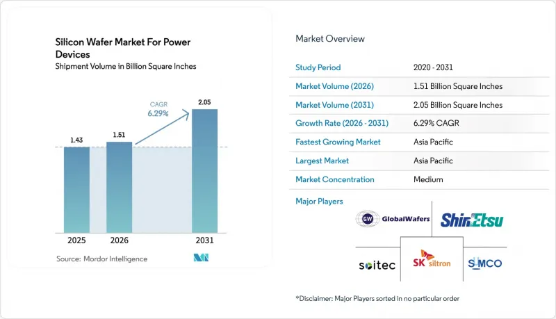
The silicon wafer market for power devices was valued at 1.43 billion square inches in 2025 and is estimated to grow from 1.51 billion square inches in 2026 to reach 2.05 billion square inches by 2031, at a 6.29% CAGR during the forecast period from 2026 to 2031.
Growth is anchored by vehicle electrification, renewable-energy grid upgrades, and the steady conversion of industrial drives from mechanical to electronic power control. Wide-bandgap materials, tighter export rules on epitaxial tools, and larger-diameter substrates are reshaping supply-chain strategies, while cost-reduction pressure is encouraging backward integration by integrated device manufacturers. The silicon wafer market is further influenced by polysilicon price swings that compress polished-wafer margins, although long-term contracts soften the impact for tier-one suppliers. Competitive intensity remains high as scale advantages in 300 mm lines converge with localization incentives in North America and Europe.
Insights and Trends of Silicon Wafer Market For Power Devices
EV-Led Demand Surge for High-Efficiency Power Conversion
Electric vehicles are shifting from 400-volt to 800-volt battery platforms, cutting fast-charge times to under 20 minutes and reducing wiring mass. SiC MOSFETs switching above 20 kHz replace multiple silicon switches, shrinking passive components and lowering total inverter cost even at a wafer premium. Automakers in China, Europe, and the United States are vertically integrating SiC device production to secure substrate supply and capture additional margin, reinforcing multi-year wafer demand growth. The International Energy Agency projects battery-electric and plug-in hybrid sales of 17 million units in 2026, which equates to roughly 50 million square inches of epitaxial SiC wafers. This demand underpins sustained expansion of the silicon wafer market across the automotive value chain.
Renewable-Energy Build-Out Driving High-Voltage Inverter Wafers
Utility-scale solar and offshore wind installations operate at direct-current bus voltages between 1,000 and 1,500 volts, pushing power-device ratings beyond 1,700 volts. In 2025 the United States added 35 GW of solar and 12 GW of wind capacity, translating into nearly 80 million square inches of high-voltage substrates for inverter modules. Emerging markets such as India are matching this trajectory through multi-gigawatt annual targets, each paired with inverter efficiency mandates that favor SiC devices. European auctions now stipulate stringent harmonic-distortion thresholds, further accelerating the adoption of thick-epi wafers with low defect densities. These policies collectively reinforce the silicon wafer market's momentum in high-voltage segments.
Polysilicon Feedstock Price Volatility
Spot polysilicon prices fell from USD 30 per kg in early 2023 to USD 6-8 per kg by late 2024, compressing polished-wafer gross margins by up to eight percentage points. Suppliers locked into higher long-term contracts faced opportunity costs when spot buyers undercut their pricing. Trade investigations on dumping added tariff uncertainty, raising procurement risk and hindering short-term planning. Although epitaxial-grade suppliers can absorb some variance through premiums, sustained volatility dampens investment appetite and can slow wafer-capacity additions in cost-sensitive segments.
Other drivers and restraints analyzed in the detailed report include:
- Shift to 300 mm Lines Lowering Cost Per Die
- Rising Industrial Automation and Electrified Factory Drives
- USD 1 Billion+ CAPEX Barrier for 200-300 mm SiC Wafer Fabs
For complete list of drivers and restraints, kindly check the Table Of Contents.
Segment Analysis
The 200 mm category retained 62.68% of the silicon wafer market for power devices in 2025, reflecting legacy fab infrastructure that remains cost-effective for medium-power devices. Yet the 300 mm class is forecast to post a 7.56% CAGR as automotive tier-ones demand larger die counts per wafer to amortize clean-room overhead. Early production runs already demonstrate 2.3-times usable die with comparable defect density, confirming that learning curves are steep enough to sustain the silicon wafer market size advantages at larger diameters.
Yield drag from thermo-mechanical bow above 50 µm still limits immediate mass adoption, but standards groups are driving thickness-variation targets below 2 µm. Back-side ion implantation and optimized epitaxy recipes are showing double-digit yield gains, suggesting that volume tipping points will arrive within four years. Scale leaders able to master bow control will hold durable cost positions across the silicon wafer market.
Epitaxial wafers captured 64.39% of the market share in 2025 on the strength of trench-gate MOSFET migration, and they are set to advance at a 7.16% CAGR. Precise doping and thickness uniformity enable lower on-resistance and higher switching speeds, attributes essential to automotive and renewable-energy power trains. Tight integration between deposition tools and AI-assisted metrology now lifts tool utilization from 75% to 85%, freeing latent capacity that underpins a resilient silicon wafer market size at the premium end.
Polished substrates remain relevant in diodes and legacy thyristors, where value thresholds are low but margin pressure is increasing due to polysilicon price shocks. Suppliers operating in both polished and epitaxial segments mitigate risks effectively. However, sustained growth is clearly shifting toward high-specification epitaxy, emphasizing its strategic importance within the broader silicon wafer market.
The Silicon Wafer Market for Power Devices Report is Segmented by Diameter (150 Mm, and More), Wafer Type (Polished, and Epitaxial), Device Type (IGBT, and More), Voltage Range (Low Voltage, Medium Voltage, and High Voltage), End-Use Industry (Automotive, Industrial and Automation, Renewable Energy and Energy Storage, and More), and Geography. The Market Forecasts are Provided in Terms of Volume (Square Inches).
Geography Analysis
Asia-Pacific commanded 69.98% of the market share in 2025 and is projected to post an 8.01% CAGR through 2031. Expansion programs by China's National Silicon Industry Group, Japan's investments in 300 mm polishing lines, and South Korea's SiC capacity additions create a formidable ecosystem that anchors the silicon wafer market. Government robotics, EV, and renewable-energy targets further reinforce regional demand, ensuring that local fabs operate near full utilization.
North America is experiencing an investment surge catalyzed by CHIPS Act incentives and automotive localization goals. New facilities in New York, North Carolina, and Texas reduce dependence on imports, diversify supply risk, and embed advanced 300 mm processes closer to end-markets. The region's policy environment, combined with access to leading semiconductor equipment suppliers, positions it as a credible secondary hub in the silicon wafer market.
Europe leverages the European Chips Act and stringent vehicle-emission rules to claim a larger share of global power-device production. Expansion projects in Germany and Italy emphasize SiC epitaxy and 300 mm silicon, supported by multi-billion-dollar public funding. Collaborative platforms focused on engineered substrates and ultra-thin wafers illustrate Europe's strategy of technology differentiation rather than cost leadership. South America and the Middle East and Africa remain import-oriented today, yet early initiatives signal long-term ambitions to establish regional substrate capabilities.
- Shin-Etsu Chemical
- SUMCO Corporation
- GlobalWafers Co., Ltd.
- Siltronic AG
- SK Siltron Co., Ltd.
- Soitec S.A.
- National Silicon Industry Group (NSIG)
- Wafer Works Corporation
- Ferrotec Holdings Corporation
- Hangzhou Lion Microelectronics
- Infineon Technologies AG
- STMicroelectronics N.V.
- onsemi
- Wolfspeed, Inc.
- ROHM Co., Ltd.
- Mitsubishi Electric Corporation
- Fuji Electric Co., Ltd.
- SKC-TankeBlue Semiconductor
- Showa Denko K.K.
- Hebei Synlight Crystal
Additional Benefits:
- The market estimate (ME) sheet in Excel format
- 3 months of analyst support
TABLE OF CONTENTS
1 INTRODUCTION
- 1.1 Study Assumptions and Market Definition
- 1.2 Scope of the Study
2 RESEARCH METHODOLOGY
3 EXECUTIVE SUMMARY
4 MARKET LANDSCAPE
- 4.1 Market Overview
- 4.2 Market Drivers
- 4.2.1 EV-Led Demand Surge for High-Efficiency Power Conversion
- 4.2.2 Renewable-Energy Build-Out Driving High-Voltage Inverter Wafers
- 4.2.3 Shift to 300 Mm Lines Lowering Cost Per Die
- 4.2.4 Rising Industrial Automation and Electrified Factory Drives
- 4.2.5 On-Wafer Back-Side Vias Enabling Ultra-Thin Automotive Modules
- 4.2.6 AI-Driven In-Situ Metrology Freeing Latent Epi Capacity
- 4.3 Market Restraints
- 4.3.1 Polysilicon Feedstock Price Volatility
- 4.3.2 USD 1 B+ CAPEX Barrier for 200-300 Mm Sic Wafer Fabs
- 4.3.3 Thermo-Mechanical Bow in 300 Mm Sic Wafers Slashing Yields
- 4.3.4 Export-Control Uncertainty for Next-Gen Epi Reactors
- 4.4 Industry Supply-Chain Analysis
- 4.5 Regulatory Landscape
- 4.6 Technological Outlook
- 4.7 Impact of Macroeconomic Factors on the Market
- 4.8 Porter's Five Forces Analysis
- 4.8.1 Threat of New Entrants
- 4.8.2 Bargaining Power of Suppliers
- 4.8.3 Bargaining Power of Buyers
- 4.8.4 Threat of Substitutes
- 4.8.5 Intensity of Competitive Rivalry
5 MARKET SIZE AND GROWTH FORECASTS (VOLUME)
- 5.1 By Diameter
- 5.1.1 150 mm
- 5.1.2 200 mm
- 5.1.3 300 mm
- 5.2 By Wafer Type
- 5.2.1 Polished
- 5.2.2 Epitaxial
- 5.3 By Device Type
- 5.3.1 IGBT
- 5.3.2 MOSFET
- 5.3.3 Diode
- 5.3.4 Thyristor
- 5.4 By Voltage Range
- 5.4.1 Low Voltage (Less than 200V)
- 5.4.2 Medium Voltage (200-650V)
- 5.4.3 High Voltage (Above 650V)
- 5.5 By End-Use Industry
- 5.5.1 Automotive
- 5.5.2 Industrial and Automation
- 5.5.3 Renewable Energy and Energy Storage
- 5.5.4 Consumer and Appliance Power
- 5.5.5 Telecom and Infrastructure Power Systems
- 5.6 By Geography
- 5.6.1 North America
- 5.6.1.1 United States
- 5.6.1.2 Canada
- 5.6.1.3 Mexico
- 5.6.2 Europe
- 5.6.2.1 Germany
- 5.6.2.2 United Kingdom
- 5.6.2.3 France
- 5.6.2.4 Rest of Europe
- 5.6.3 Asia-Pacific
- 5.6.3.1 China
- 5.6.3.2 Japan
- 5.6.3.3 India
- 5.6.3.4 South Korea
- 5.6.3.5 Taiwan
- 5.6.3.6 Rest of Asia-Pacific
- 5.6.4 South America
- 5.6.5 Middle East and Africa
- 5.6.1 North America
6 COMPETITIVE LANDSCAPE
- 6.1 Market Concentration
- 6.2 Strategic Moves
- 6.3 Market Share Analysis
- 6.4 Company Profiles (includes Global level Overview, Market Level Overview, Core Segments, Financials as Available, Strategic Information, Market Rank/Share for Key Companies, Products and Services, and Recent Developments)
- 6.4.1 Shin-Etsu Chemical
- 6.4.2 SUMCO Corporation
- 6.4.3 GlobalWafers Co., Ltd.
- 6.4.4 Siltronic AG
- 6.4.5 SK Siltron Co., Ltd.
- 6.4.6 Soitec S.A.
- 6.4.7 National Silicon Industry Group (NSIG)
- 6.4.8 Wafer Works Corporation
- 6.4.9 Ferrotec Holdings Corporation
- 6.4.10 Hangzhou Lion Microelectronics
- 6.4.11 Infineon Technologies AG
- 6.4.12 STMicroelectronics N.V.
- 6.4.13 onsemi
- 6.4.14 Wolfspeed, Inc.
- 6.4.15 ROHM Co., Ltd.
- 6.4.16 Mitsubishi Electric Corporation
- 6.4.17 Fuji Electric Co., Ltd.
- 6.4.18 SKC-TankeBlue Semiconductor
- 6.4.19 Showa Denko K.K.
- 6.4.20 Hebei Synlight Crystal
7 MARKET OPPORTUNITIES AND FUTURE OUTLOOK
- 7.1 White-space and Unmet-Need Assessment

