
PUBLISHER: Mordor Intelligence | PRODUCT CODE: 2044016

PUBLISHER: Mordor Intelligence | PRODUCT CODE: 2044016
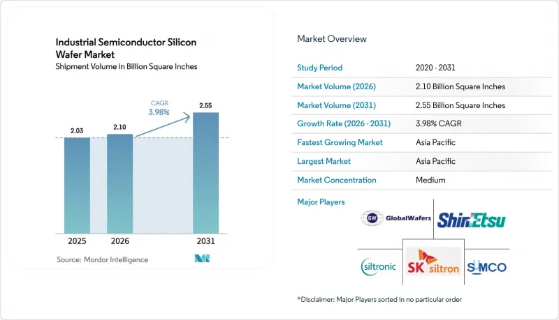
Industrial Semiconductor Silicon Wafer - Market Share Analysis, Industry Trends & Statistics, Growth Forecasts (2026 - 2031)
The industrial semiconductor silicon wafer market size is projected to expand from 2.03 billion square inches in 2025 and 2.10 billion square inches in 2026 to 2.55 billion square inches by 2031, registering a CAGR of 3.98% between 2026 and 2031.
Most of the incremental area will come from 300 mm substrates, which already account for nearly half of total consumption, while 200 mm epitaxial wafers for silicon-carbide (SiC) power devices and silicon-on-insulator (SOI) wafers for photonics accelerate their mix gains. A rebound in memory spending, tighter flatness requirements for gate-all-around logic, and inventory normalization in 2025 have together lifted shipment momentum. China's record wafer investments, Europe's push for supply-chain resilience, and the United States' CHIPS Act subsidies are reshaping capacity decisions, often overriding pure cost considerations. Helium price spikes, 200 mm tool obsolescence, and packaging-induced warpage remain the chief operational risks. Meanwhile, incumbents use AI-based crystal-growth controls and reclaim initiatives to offset cost pressure and preserve margins.
Global Industrial Semiconductor Silicon Wafer Market Trends and Insights
Rising EV Penetration And Shift Toward 800-V Vehicle Platforms
Battery-electric models are migrating from 400-V to 800-V systems, which cuts charging time and wiring weight, but requires SiC MOSFETs processed on 200 mm epitaxial wafers. Infineon boosted 200 mm SiC yields by nearly 85% in 2024 through AI-optimized crystal growth, letting the firm double output without proportional capex. Wolfspeed achieved a 30% cost reduction in 200 mm SiC wafers that same year, widening the price gap with legacy silicon devices. Chinese brands BYD and NIO adopted 800 V early, locking in domestic substrate supply and extending global lead times beyond 26 weeks. Tight 200 mm availability is therefore an outgrowth of the EV transition and not merely a cyclical inventory issue.
Rapid Build-Out Of 800 V Charging Infrastructure
The European Alternative Fuels Infrastructure Regulation mandates high-power chargers every 60 km along core corridors by 2025, triggering more than 50,000 ultra-fast installations in 2024-2025.China's State Grid commissioned over 100,000 new 350 kW ports in 2025, each power module containing multiple SiC or GaN die. Charging-equipment makers such as ABB sign multiyear 200 mm wafer contracts to protect supply, further straining the spot market and reinforcing demand visibility.
Limited Availability Of 200 MM Substrates
Toolmakers have largely frozen new 200 mm equipment development, so fabs depend on refurbished lines with longer lead times, locking in a structural shortage. Okmetic's 50,000-wafer capacity addition in Finland adds less than 2% to global demand and fails to ease 26-week automotive waits. As large IDMs migrate analog workloads to 300 mm, niche players face even tighter allocations.
Other drivers and restraints analyzed in the detailed report include:
- High-Temperature, High-Frequency Advantages Over Silicon
- Government Incentives For Wide-Band-Gap Fabs
- Capital-Intensive Crystal-Growth Equipment
For complete list of drivers and restraints, kindly check the Table Of Contents.
Segment Analysis
The 300 mm portion of the industrial semiconductor silicon wafer market size commanded 48.62% in 2025 and is on track for a 4.85% CAGR as leading logic and memory fabs seek larger die counts per pass. Samsung and SK Hynix dedicated more than one-fifth of their DRAM starts to high-bandwidth memory in 2026, accelerating consumption of 300 mm blanks. Even analog IDMs now explore 300 mm conversions to escape 200 mm bottlenecks.
Smaller diameters retain relevance in RF, sensors, and optoelectronics where legacy tools suffice and capex is modest. However, hybrid bonding and through-silicon-via packaging demand the flatness tolerance achievable only on 300 mm substrates, effectively locking many advanced programs into the larger format. Chinese suppliers, led by National Silicon Industry Group, funnel fresh funding into commodity 300 mm grades, adding over 1 million wafers a month and challenging Japanese dominance.
The Industrial Semiconductor Silicon Wafer Market Report is Segmented by Wafer Diameter (Up To 150 Mm, 200 Mm, and 300 Mm), Semiconductor Device Type (Logic, Memory, Analog, and More), Wafer Type (Prime Polished, Epitaxial, SOI, and Specialty Silicon), and Geography (North America, Europe, Asia-Pacific, South America, Middle East, Africa). The Market Forecasts are Provided in Terms of Volume (Square Inches).
Geography Analysis
Asia-Pacific represented 82.39% of worldwide consumption in 2025, and its 4.15% CAGR keeps the region firmly atop the industrial semiconductor silicon wafer market. China alone spent CNY 455 billion (USD 63.3 billion) on front-end capacity in 1H 2025, funneling more than half into substrates. Taiwan focuses on leading-edge logic, South Korea on memory, and Japan on wide-band-gap and SOI pilot lines.
North America remains smaller but grows quickly as CHIPS Act money underwrites GlobalWafers' USD 3.5 billion Texas fab, with an additional USD 4 billion expansion announced the same year. SK Siltron's Michigan site, budgeted at USD 3.6 billion, will bring fresh 300 mm capacity by 2027. Canada and Mexico handle backend steps, which in turn drive demand for reclaimed or test wafers.
Europe stabilizes its share through the EUR 43 billion (USD 47.3 billion) Chips Act, supporting Siltronic's EUR 2 billion (USD 2.2 billion) Fab-Next in Singapore for dual-region customers. Germany and France emphasize analog and power sovereignty, prolonging 200 mm relevance despite global 300 mm migration. Other regions together hold under 2% share but explore SiC initiatives tied to renewable power ambitions.
- Shin-Etsu Chemical Co., Ltd.
- SUMCO Corporation
- GlobalWafers Co., Ltd.
- Siltronic AG
- SK Siltron Co., Ltd.
- Soitec SA
- Okmetic Oy
- Wafer Works Corp.
- National Silicon Industry Group (NSIG)
- Zhonghuan Advanced Semiconductor Materials
- QL Electronics
- Nanjing Guosheng Electronics
- Hebei Puxing Electronic Technology
- Shanghai Advanced Silicon Technology (AST)
- Ferrotec Holdings Corporation
- Topsil Semiconductor Materials
- Retain GlobalWafers Co.,
- Simgui
- GRINM Semiconductor Materials
- ESWIN Technology Group
- Formosa Sumco Technology Corp.
Additional Benefits:
- The market estimate (ME) sheet in Excel format
- 3 months of analyst support
TABLE OF CONTENTS
1 INTRODUCTION
- 1.1 Study Assumptions and Market Definition
- 1.2 Scope of the Study
2 RESEARCH METHODOLOGY
3 EXECUTIVE SUMMARY
4 MARKET LANDSCAPE
- 4.1 Market Overview
- 4.2 Industry Value-Chain Analysis
- 4.3 Regulatory Landscape
- 4.4 Technological Outlook
- 4.5 Impact of Macroeconomic Factors on the Market
- 4.6 Porter's Five Forces Analysis
- 4.6.1 Bargaining Power of Suppliers
- 4.6.2 Bargaining Power of Buyers
- 4.6.3 Threat of New Entrants
- 4.6.4 Threat of Substitutes
- 4.6.5 Intensity of Competitive Rivalry
- 4.7 Market Drivers
- 4.7.1 Rising EV Penetration and Shift Toward 800-V Vehicle Platforms
- 4.7.2 Rapid Build-Out of 800 V Charging Infrastructure
- 4.7.3 High-Temperature, High-Frequency Performance Advantages over Si
- 4.7.4 Government Incentives for Wide-Band-Gap Fabs
- 4.7.5 AI-Driven Demand for 3D-IC Silicon Photonics Requiring Ultra-Flat SOI Wafers
- 4.7.6 Wafer Reclaim And Circular-Economy Mandates Lowering Total Cost-of-Ownership for 300 mm Lines
- 4.8 Market Restraints
- 4.8.1 Limited Availability of 200 mm Substrates
- 4.8.2 Capital-Intensive Crystal-Growth Equipment
- 4.8.3 Packaging-Induced Thermo-Mechanical Stress
- 4.8.4 Looming Helium Supply Constraints Impacting CMP and Epitaxial Tools
5 MARKET SIZE And GROWTH FORECASTS (VOLUME)
- 5.1 By Wafer Diameter
- 5.1.1 Up to 150 mm
- 5.1.2 200 mm
- 5.1.3 300 mm
- 5.2 By Semiconductor Device Type
- 5.2.1 Logic
- 5.2.2 Memory
- 5.2.3 Analog
- 5.2.4 Discrete
- 5.2.5 Other Semiconductor Device Types (Optoelectronics, Sensors, Micro)
- 5.3 By Wafer Type
- 5.3.1 Prime Polished
- 5.3.2 Epitaxial
- 5.3.3 Silicon-on-Insulator (SOI)
- 5.3.4 Specialty Silicon (High-Resistivity, Power, Sensor-Grade)
- 5.4 By Geography
- 5.4.1 North America
- 5.4.1.1 United States
- 5.4.1.2 Canada
- 5.4.1.3 Mexico
- 5.4.2 Europe
- 5.4.2.1 Germany
- 5.4.2.2 United Kingdom
- 5.4.2.3 France
- 5.4.2.4 Rest of Europe
- 5.4.3 Asia-Pacific
- 5.4.3.1 China
- 5.4.3.2 Japan
- 5.4.3.3 India
- 5.4.3.4 South Korea
- 5.4.3.5 Taiwan
- 5.4.3.6 Rest of Asia-Pacific
- 5.4.4 South America
- 5.4.5 Middle East
- 5.4.6 Africa
- 5.4.1 North America
6 COMPETITIVE LANDSCAPE
- 6.1 Market Concentration
- 6.2 Strategic Moves
- 6.3 Market Share Analysis
- 6.4 Company Profiles (includes Global Level Overview, Market Level Overview, Core Segments, Financials as available, Strategic Information, Market Rank/Share, Products And Services, Recent Developments)
- 6.4.1 Shin-Etsu Chemical Co., Ltd.
- 6.4.2 SUMCO Corporation
- 6.4.3 GlobalWafers Co., Ltd.
- 6.4.4 Siltronic AG
- 6.4.5 SK Siltron Co., Ltd.
- 6.4.6 Soitec SA
- 6.4.7 Okmetic Oy
- 6.4.8 Wafer Works Corp.
- 6.4.9 National Silicon Industry Group (NSIG)
- 6.4.10 Zhonghuan Advanced Semiconductor Materials
- 6.4.11 QL Electronics
- 6.4.12 Nanjing Guosheng Electronics
- 6.4.13 Hebei Puxing Electronic Technology
- 6.4.14 Shanghai Advanced Silicon Technology (AST)
- 6.4.15 Ferrotec Holdings Corporation
- 6.4.16 Topsil Semiconductor Materials
- 6.4.17 Retain GlobalWafers Co.,
- 6.4.18 Simgui
- 6.4.19 GRINM Semiconductor Materials
- 6.4.20 ESWIN Technology Group
- 6.4.21 Formosa Sumco Technology Corp.
7 MARKET OPPORTUNITIES AND FUTURE OUTLOOK
- 7.1 White-Space and Unmet-Need Assessment

