PUBLISHER: Information Network | PRODUCT CODE: 1478712

PUBLISHER: Information Network | PRODUCT CODE: 1478712
LED and OLED Lighting: Market Analysis and Manufacturing Trends
In the rapidly evolving landscape of lighting technology, LED (Light Emitting Diode) and OLED (Organic Light Emitting Diode) lighting stand at the forefront, heralding a new era of efficiency, sustainability, and design flexibility. The "LED and OLED Lighting: Market Analysis and Manufacturing Trends" report offers an in-depth exploration of these two pivotal technologies, providing a comprehensive overview of their current market status, growth trajectories, and the technological innovations that drive them.
As the global push towards energy efficiency and reduced carbon footprints intensifies, LED and OLED lighting solutions have emerged as pivotal players. Their unique attributes-notably, their energy efficiency, longer lifespans, and superior light quality-have propelled them into the spotlight, not just as alternatives to traditional lighting solutions, but as the preferred choice in a wide range of applications, from residential and commercial to industrial and architectural.
This report begins by dissecting the market dynamics of the LED and OLED sectors, analyzing key growth drivers, challenges, and opportunities. It delves into the regulatory frameworks and environmental mandates across different regions that have been instrumental in shaping the market landscape, highlighting how policy shifts are influencing demand patterns and technological advancements.

Technological innovation remains at the heart of LED and OLED development, with ongoing research and development efforts pushing the boundaries of what's possible in lighting technology. The report examines the latest advancements in material science, including novel phosphors and organic materials, that are enhancing the performance and efficiency of LED and OLED lights. It also explores the evolution of design trends, from the miniaturization of components to the integration of smart technology, which are expanding the applications and appeal of these lighting solutions.
The manufacturing landscape for LED and OLED technologies is also a focal point of this report. It assesses the impact of global supply chains, the role of economies of scale, and the strategic moves by leading manufacturers as they navigate the complexities of production, from cost considerations to the adoption of sustainable manufacturing practices.
Furthermore, the report provides a detailed analysis of the competitive environment, identifying key players, their market positioning, and strategies for innovation and growth. It also offers insights into the emerging markets and sectors that represent growth opportunities for LED and OLED technologies, including automotive lighting, horticultural applications, and wearable electronics.
Looking ahead, the report forecasts the future directions of the LED and OLED markets, considering factors such as potential technological breakthroughs, emerging economic trends, and shifts in consumer preferences. It identifies challenges that could impede growth, such as material shortages or competitive pressures, and opportunities that could fuel expansion, such as the increasing demand for smart and connected lighting systems.
In conclusion, the "LED and OLED Lighting: Market Analysis and Manufacturing Trends" report serves as an essential resource for stakeholders across the lighting industry spectrum, offering strategic insights and actionable intelligence to navigate the complexities of the market, leverage emerging opportunities, and shape the future of lighting technology.
Trends in LED and OLED Lighting

The lighting industry is undergoing a significant transformation, driven by the rapid advancements and adoption of LED (Light Emitting Diode) and OLED (Organic Light Emitting Diode) technologies. These shifts are not only changing the way spaces are illuminated but also how lighting solutions are designed, manufactured, and integrated into the modern digital ecosystem.
The key trends shaping the LED and OLED lighting markets include:
- Energy Efficiency and Sustainability: As global awareness and regulations around energy conservation and environmental sustainability intensify, LED and OLED lights, known for their low power consumption and long service life, are becoming increasingly popular. These technologies are central to green building designs and energy-saving initiatives across residential, commercial, and industrial applications.
- Smart and Connected Lighting: The integration of LED and OLED lighting with IoT (Internet of Things) technologies is a growing trend. Smart lighting systems, capable of being controlled via smartphones or voice-activated devices, are becoming commonplace in smart homes and cities. These systems offer not just convenience but also efficiency, as they can adjust lighting based on presence, ambient light levels, or time of day.
- Human-Centric and Health-Focused Lighting: There is an increasing focus on the impact of lighting on human health and well-being. LED and OLED technologies allow for the creation of lighting solutions that mimic natural light patterns, potentially improving sleep cycles, mood, and productivity. This trend is gaining traction in both residential settings and workplaces.
- Innovative Design and Flexibility: OLED technology, in particular, allows for flexible, thin, and even transparent lighting panels that can be integrated into various surfaces and materials. This opens up new avenues for innovative lighting designs and applications, from architectural features to wearable technology.
- Advancements in Light Quality and Color Rendering: Continuous improvements in LED and OLED technologies have led to better color rendering and the ability to produce a wide spectrum of light. This not only enhances the aesthetic appeal of illuminated spaces but also finds applications in sectors such as retail, where accurate color representation is critical.
- Decreasing Costs and Increasing Accessibility: As manufacturing processes mature and economies of scale are achieved, the costs of LED and OLED lighting solutions continue to decrease. This trend is making these technologies more accessible to a broader market, driving their adoption in regions and sectors where cost was previously a barrier.
- Growth in Automotive and Specialty Applications: Beyond traditional lighting, LEDs and OLEDs are increasingly used in automotive lighting, including headlights, interior lights, and displays, as well as in specialized applications such as horticultural lighting, where specific light spectra can enhance plant growth.
Table of Contents
Chapter 1. Introduction
Chapter 2. Recent Progress in High Brightness LED Technology and Applications
- 2.1. LED: Theory of Operation
- 2.2. Intellectual Property Map
- 2.3. LED Manufacturing Technologies & Costs
- 2.4. LED Market General Illumination
Chapter 3. Processing Equipment
- 3.1. Introduction
- 3.2. Deposition
- 3.2.1. MOCVD for SSL - Productivity Challenges and Solutions
- 3.2.2. Low temperature Remote Plasma Chemical Vapor Deposition (RPCVD)
- 3.3. Chemical Mechanical Planarization
- 3.4. Defect Inspection and Testing
- 3.5. Lithography
- 3.5.1. Steppers
Chapter 4. Materials of Construction
- 4.1. Introduction
- 4.2. GaN-based LED for General Lighting
- 4.2.1. Methods to Improve White LED Efficiency
- 4.2.2. Time-to-Market for LED substrates
- 4.3. LED Phosphor Manufacturing Issues
- 4.3.1. Current LED Phosphor Manufacturing
- 4.3.2. LED Phosphor Cost
Chapter 5. Packaging and Assembly Issues for High Brightness LEDs
- 5.1. Packaging for HB LEDs
- 5.1.1. Bonding
- 5.1.2. Die/Ball Bonding
- 5.1.3. Scribing
- 5.2. Wafer Level Packaging HB LEDs
- 5.3. Thermal Issues
- 5.4. Test and Inspection
Chapter 6. National Programs As Innovation Drivers
- 6.1. DOE Solid-State Lighting Manufacturing Initiative
- 6.2. DOE Solid-State Lighting Program Mission and Goal
- 6.3. Major National Research Programs Pertaining to LEDs
- 6.4. Challenges Facing SSL Manufacturing
Chapter 7. OLED Lighting
- 7.1. Opportunities for Luminaire Manufacturers
- 7.2. How Does an OLED Work
- 7.3. Differences Between OLED Lighting and OLED Display
- 7.4. Benefits of OLED Lighting Technology
- 7.5. OLED Performance Metrics
Chapter 8. OLED Manufacturing
- 8.1. Deposition Equipment and Processes for OLED Lighting
- 8.1.1. Vacuum Deposition Or Vacuum Thermal Evaporation (VTE)
- 8.1.2. Organic Vapor Deposition (OVPD)
- 8.1.3. Inkjet Printing
- 8.1.4. Roll-to-Roll (R2R)
- 8.2. General OLED Manufacturing Cost Considerations
- 8.3. Lithography
- 8.4. Substrates and Encapsulation
- 8.4.1. Substrate and Encapsulation Material Selection
- 8.4.2. Substrate Coatings
- 8.4.3. Transparent Electrodes
- 8.4.4. Encapsulation
- 8.5. Inspection and Quality Control
Chapter 9. Outlook for the Worldwide OLED Market
- 9.1. Introduction
- 9.2. Passive Matrix Capacity and Demand
- 9.3. Active Matrix Capacity and Demand
- 9.4. Cost Challenges for OLED Lighting
Chapter 10. Outlook for the Worldwide High-Brightness LED Market
- 10.1. HB LED Technology
- 10.2. HB LED Market Overview and trends
- 10.2.1. Market Drivers for SSL
- 10.2.2. LED Backlights for Notebook PCs
- 10.2.3. LED Backlights for LCD TVs
- 10.2.4. LED Backlights for Other Applications
- 10.2.5. LED Lighting Market
- 10.2.6. LED Active Outdoor Display Market
- 10.2.7. LED Signal Market
- 10.2.8. LED Automotive Market
- 10.2.9. LED Mobile Market
List of Tables
- 2.1. Color, Wavelength Material Of LED
- 2.2. Light Source Comparison
- 2.3. Comparison of LED, HB-LED, UHB-LED Characteristics
- 3.1. Epitaxy Metrics from Initial Solid-State Lighting Manufacturing R&D Roadmap
- 3.2. Process Control Metrics
- 4.1. Production Method for Various LEDs
- 4.2. LED Cost Model: Impact of Substrate Choice
- 4.3. Comparison of $/klm for LED Made on Various 2" Substrates
- 5.1. Properties of Die Bonding Processes
- 7.1. Efficiency of Emitter Materials
- 7.2. Status of Technology Towards Lighting Targets
- 7.3. Cost Targets for Panels
- 7.4. Cost Comparison OLED Display vs Lighting
- 8.1. Cost Targets for Panels Produced by Traditional Methods
- 10.1. Forecast of LED Backlights for Notebook PCs
- 10.2. Forecast of LED Backlights for LCD TVs
- 10.3. Forecast of LED Backlights for Other Application
- 10.4. Forecast of LED Lighting Market
- 10.5. Forecast of LED Active Outdoor Display Market
- 10.6. Forecast of LED Signal Market
- 10.7. Forecast of LED Automotive Market
- 10.8. Forecast of LED Mobile Market
- 10.9. Top 10. LED Vendors
List of Figures
- 2.1. Operation of LED
- 2.2. Key Intellectual Property Relationships
- 2.3. DOE Roadmap
- 2.4. Relative Manufacturing Costs
- 2.5. Pareto Analysis Of SSL Manufacturing Costs
- 2.6. Market drivers for LED Biz and Applications
- 2.7. SSL vs. Classical Technologies
- 2.8. LED Performance vs. Traditional Light Sources
- 2.9. Energy Production and Use Comparison
- 2.10. Worldwide LED Market Forecast
- 3.1. SSL - LED manufacturing with MOCVD: productivity and Cost Analysis
- 3.2. Larger Wafer Size: GaN LEDs
- 3.3. Global Shipments of MOCVD Tools By Vendor
- 3.4. Global Shipments of MOCVD Tools By Region
- 3.5. Diagram of RPCVD Reactor
- 3.6. Comparison between MOCVD and RPCVD
- 3.7. CMP Process
- 3.8. Nanoimprint Lithography System
- 3.9. The Phlatlight Chip
- 4.1. Regular LED (white) Front-End Steps
- 4.2. Current Blocking Layer
- 4.3. Regular LED (white) Production Costs for 100k wafers/year
- 4.4. HB LED (white) Production Costs for 100k wafers/year
- 4.5. Main Manufacturing Steps for GaN-based LED
- 4.6. Regular LED (white) Back-End
- 4.7. Methods to Improve White LED Efficiency
- 4.8. Phosphor Coating - Four Approaches
- 5.1. Hybrid Integration Approach to HD-LED Package
- 5.2. Chain Wire Bond
- 5.3. HB-LED with Silicon Carrier Submount
- 5.4. Silicon interposer for MEMS / LED Applications
- 5.5. High Brightness LED
- 5.6. SMD Package Cost Structure
- 5.7. Packaging Changes Result in Optical Improvements
- 5.8. Substrate Solutions for HB/HP LEDs
- 6.1. DOE Solid-State Lighting Program Strategy
- 6.2. DOE Efficacy Targets
- 6.3. Congressional Appropriations
- 6.4. SSL R&D Project Funding
- 6.5. Price Targets
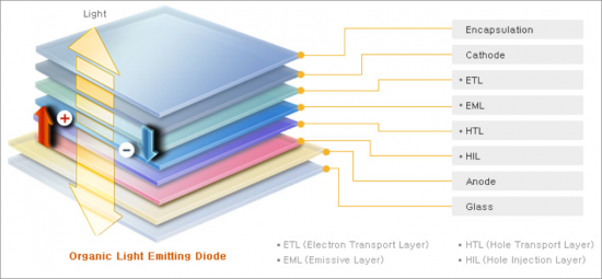
- 7.1. OLED Lighting Stack
- 8.1. Schematic of VTE Deposition System
- 8.2. Schematic of OVPD Deposition System
- 8.3. Comparison Between VTE and OVPD Technology
- 8.4. Schematic of Inkjet Deposition System
- 8.5. Schematic of R2R Deposition System
- 8.6. Illustration of Planarization Layer on OLED
- 9.1. Schematic of PMOLED
- 9.2. PMOLED Stack/Driving Architecture
- 9.3. Schematic of AMOLED
- 9.4. Passive Matrix OLED Capacity and Demand
- 9.5. Active Matrix OLED Capacity and Demand
- 10.1. LED Market by Sector
- 10.2. Worldwide LED Market Forecast


