
PUBLISHER: Global Market Insights Inc. | PRODUCT CODE: 1928874

PUBLISHER: Global Market Insights Inc. | PRODUCT CODE: 1928874
Thin Wafer Processing and Dicing Equipment Market Opportunity, Growth Drivers, Industry Trend Analysis, and Forecast 2026 - 2035
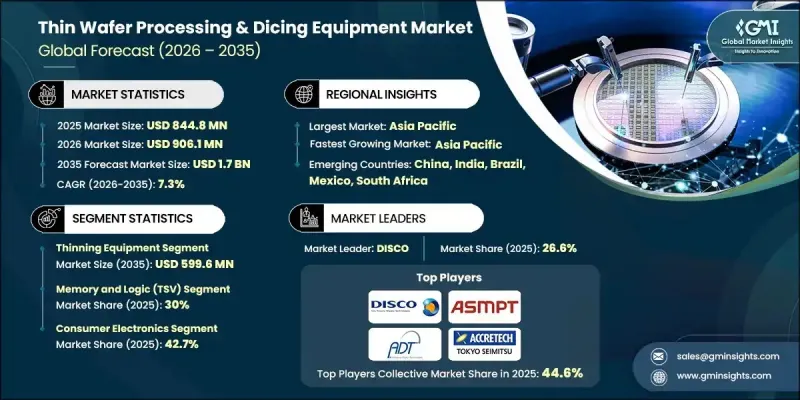
The Global Thin Wafer Processing & Dicing Equipment Market was valued at USD 844.8 million in 2025 and is estimated to grow at a CAGR of 7.3% to reach USD 1.7 billion by 2035.
Market growth is supported by the rising complexity of semiconductor devices and the need for higher precision during backend manufacturing. Increasing demand for thinner, lighter, and more reliable components continues to reshape equipment requirements across the value chain. Advancements in device architecture and materials place greater emphasis on accuracy, yield improvement, and reduced material stress. Equipment suppliers respond by delivering advanced solutions that enable precise wafer thinning and separation while maintaining structural integrity. The adoption of next-generation packaging approaches further intensifies demand for high-precision processes. Manufacturers prioritize productivity, cost efficiency, and process stability to support large-scale semiconductor production. Automation and intelligent systems play an expanding role in improving throughput, reducing downtime, and enhancing quality control. Together, these factors establish thin wafer processing and dicing equipment as a critical enabler of innovation and scalability within the global semiconductor industry.
| Market Scope | |
|---|---|
| Start Year | 2025 |
| Forecast Year | 2026-2035 |
| Start Value | $844.8 Million |
| Forecast Value | $1.7 Billion |
| CAGR | 7.3% |
Equipment suppliers continue to advance non-contact and low-stress processing technologies to improve yields and support increasingly fragile wafer structures. Greater focus on dimensional accuracy, surface quality, and operational efficiency reflects broader industry trends toward higher device density. Automation and data-driven systems support improved process control, defect reduction, and predictive maintenance across manufacturing lines.
The thinning equipment segment is expected to reach USD 599.6 million by 2035. Demand rises as semiconductor producers move toward ultra-thin wafers to support compact and high-performance devices. Ongoing improvements in precision processing techniques contribute to better yield rates, lower stress levels, and enhanced compatibility with delicate wafers used in advanced device fabrication.
The MEMS devices segment is forecast to grow at a CAGR of 8.6% between 2026 and 2035. Growth is driven by expanding adoption across multiple end-use industries that require compact, reliable, and high-precision components. Increased use of ultra-thin wafer handling and advanced separation technologies improves consistency and reliability. Automation and real-time monitoring systems further support yield optimization.
Europe Thin Wafer Processing & Dicing Equipment Market accounted for USD 161.4 million in 2025 and is expected to record strong growth through the forecast period. Regional demand is supported by continued investment in advanced semiconductor manufacturing, particularly for high-performance and precision-driven applications across multiple industries.
Key companies active in the Global Thin Wafer Processing & Dicing Equipment Market include DISCO Corporation, Lam Research Corporation, ASMPT, KLA Corporation, EV Group (EVG), Han's Laser Technology Co., Ltd., Advanced Dicing Technologies, HANMI Semiconductor, AXUS TECHNOLOGY, Dynatex International, Citizen Chiba Precision Co., Ltd., and Lam Research Corporation. Companies operating in the Global Thin Wafer Processing & Dicing Equipment Market focus on strengthening their competitive position through technology innovation and product differentiation. Investment in research and development remains a core strategy to improve precision, yield, and compatibility with advanced semiconductor designs. Manufacturers expand automation and intelligent software integration to enhance productivity and reduce operational risks.
Table of Contents
Chapter 1 Methodology and Scope
- 1.1 Market scope and definition
- 1.2 Research design
- 1.2.1 Research approach
- 1.2.2 Data collection methods
- 1.3 Data mining sources
- 1.3.1 Global
- 1.3.2 Regional/Country
- 1.4 Base estimates and calculations
- 1.4.1 Base year calculation
- 1.4.2 Key trends for market estimation
- 1.5 Primary research and validation
- 1.5.1 Primary sources
- 1.6 Forecast model
- 1.7 Research assumptions and limitations
Chapter 2 Executive Summary
- 2.1 Industry 360° synopsis, 2021 - 2034
- 2.2 Key market trends
- 2.2.1 Equipment type trends
- 2.2.2 Wafer size trends
- 2.2.3 Wafer thickness trends
- 2.2.4 Application trends
- 2.2.5 End-use industry trends
- 2.2.6 Regional trends
- 2.3 TAM analysis, 2025-2034
- 2.4 CXO perspectives: Strategic imperatives
- 2.4.1 Executive decision points
- 2.4.2 Critical success factors
- 2.5 Future outlook and strategic recommendations
Chapter 3 Industry Insights
- 3.1 Industry ecosystem analysis
- 3.1.1 Supplier landscape
- 3.1.2 Profit margin analysis
- 3.1.3 Cost structure
- 3.1.4 Value addition at each stage
- 3.1.5 Factor affecting the value chain
- 3.1.6 Disruptions
- 3.2 Industry impact forces
- 3.2.1 Growth drivers
- 3.2.1.1 Rising demand for miniaturized electronic devices
- 3.2.1.2 Proliferation of 5G and high-performance computing applications
- 3.2.1.3 Increased use of advanced semiconductor materials
- 3.2.1.4 Growth in automotive electronics and EVs
- 3.2.2 Industry pitfalls and challenges
- 3.2.2.1 High costs of advanced dicing equipment
- 3.2.2.2 Increased fragility of thinned wafers
- 3.2.3 Market opportunities
- 3.2.3.1 Integration of artificial intelligence and automation in wafer handling
- 3.2.3.2 Growth in MEMS, optical, and RF device manufacturing
- 3.2.1 Growth drivers
- 3.3 Growth potential analysis
- 3.4 Regulatory landscape
- 3.4.1 North America
- 3.4.2 Europe
- 3.4.3 Asia Pacific
- 3.4.4 Latin America
- 3.4.5 Middle East & Africa
- 3.5 Porter';s analysis
- 3.6 PESTEL analysis
- 3.7 Technology and innovation landscape
- 3.7.1 Current technological trends
- 3.7.2 Emerging technologies
- 3.8 Emerging business models
- 3.9 Compliance requirements
- 3.10 Patent and IP analysis
- 3.11 Geopolitical and trade dynamics
Chapter 4 Competitive Landscape, 2024
- 4.1 Introduction
- 4.2 Company market share analysis
- 4.2.1 By region
- 4.2.1.1 North America
- 4.2.1.2 Europe
- 4.2.1.3 Asia Pacific
- 4.2.1.4 Latin America
- 4.2.1.5 Middle East & Africa
- 4.2.1 By region
- 4.3 Competitive benchmarking of key players
- 4.3.1 Financial performance comparison
- 4.3.1.1 Revenue
- 4.3.1.2 Profit margin
- 4.3.1.3 R&D
- 4.3.2 Product portfolio comparison
- 4.3.2.1 Product range breadth
- 4.3.2.2 Technology
- 4.3.2.3 Innovation
- 4.3.3 Geographic presence comparison
- 4.3.3.1 Global footprint analysis
- 4.3.3.2 Service network coverage
- 4.3.3.3 Market penetration by region
- 4.3.4 Competitive positioning matrix
- 4.3.4.1 Leaders
- 4.3.4.2 Challengers
- 4.3.4.3 Followers
- 4.3.4.4 Niche players
- 4.3.5 Strategic outlook matrix
- 4.3.1 Financial performance comparison
- 4.4 Key developments, 2021-2024
- 4.4.1 Mergers and acquisitions
- 4.4.2 Partnerships and collaborations
- 4.4.3 Technological advancements
- 4.4.4 Expansion and investment strategies
- 4.4.5 Digital transformation initiatives
- 4.5 Emerging/ startup competitors landscape
Chapter 5 Market Estimates and Forecast, By Equipment Type, 2022 - 2035 ($ Mn)
- 5.1 Key trends
- 5.2 Thinning equipment
- 5.3 Dicing equipment
- 5.3.1 Blade dicing
- 5.3.2 Laser dicing
- 5.3.3 Stealth dicing
- 5.3.4 Plasma dicing
- 5.4 Handling & support equipment
- 5.4.1 Temporary bonding/debonding systems
- 5.4.2 Wafer mounting/demounting systems
- 5.4.3 Cleaning & inspection systems
Chapter 6 Market Estimates and Forecast, By Wafer Size, 2022 - 2035 ($ Mn)
- 6.1 Key trends
- 6.2 Less than 4 inch
- 6.3 5 inch and 6 inch
- 6.4 8 inch
- 6.5 12 inch
Chapter 7 Market Estimates and Forecast, By Wafer Thickness, 2022 - 2035 ($ Mn)
- 7.1 Key trends
- 7.2 750 µm (standard / less thin)
- 7.3 120 µm (advanced mainstream)
- 7.4 50 µm and below
Chapter 8 Market Estimates and Forecast, By Application, 2022 - 2035 ($ Mn)
- 8.1 Key trends
- 8.2 CMOS image sensors
- 8.3 Memory and logic (TSV)
- 8.4 MEMS device
- 8.5 Power device
- 8.6 RFID
- 8.7 Others
Chapter 9 Market Estimates and Forecast, By End Use Industry, 2022 - 2035 ($ Mn)
- 9.1 Key trends
- 9.2 Consumer electronics
- 9.3 Automotive
- 9.4 Telecommunications
- 9.5 Healthcare
- 9.6 Aerospace & defense
- 9.7 Industrial
- 9.8 Others
Chapter 10 Market Estimates and Forecast, By Region, 2022 - 2035 ($ Mn)
- 10.1 Key trends
- 10.2 North America
- 10.2.1 U.S.
- 10.2.2 Canada
- 10.3 Europe
- 10.3.1 Germany
- 10.3.2 UK
- 10.3.3 France
- 10.3.4 Spain
- 10.3.5 Italy
- 10.3.6 Netherlands
- 10.4 Asia Pacific
- 10.4.1 China
- 10.4.2 India
- 10.4.3 Japan
- 10.4.4 Australia
- 10.4.5 South Korea
- 10.5 Latin America
- 10.5.1 Brazil
- 10.5.2 Mexico
- 10.5.3 Argentina
- 10.6 Middle East and Africa
- 10.6.1 South Africa
- 10.6.2 Saudi Arabia
- 10.6.3 UAE
Chapter 11 Company Profiles
- 11.1 Global Key Players
- 11.1.1 DISCO Corporation
- 11.1.2 ASMPT
- 11.1.3 KLA Corporation
- 11.1.4 Lam Research Corporation
- 11.2 Regional Key Players
- 11.2.1 North America
- 11.2.1.1 Plasma-Therm
- 11.2.1.2 SPTS Technologies Ltd.
- 11.2.1.3 Loadpoint Ltd.
- 11.2.2 Europe
- 11.2.2.1 Synova SA
- 11.2.2.2 Modutek Corporation
- 11.2.2.3 Dynatex International
- 11.2.3 APAC
- 11.2.3.1 Tokyo Electron Limited
- 11.2.3.2 TOKYO SEIMITSU CO., LTD (Accretech)
- 11.2.3.3 Panasonic Connect Co., Ltd.
- 11.2.1 North America
- 11.3 Niche Players / Disruptors
- 11.3.1 Advanced Dicing Technologies
- 11.3.2 AXUS TECHNOLOGY
- 11.3.3 Citizen Chiba Precision Co., Ltd.
- 11.3.4 HANMI Semiconductor
- 11.3.5 Han's Laser Technology Co., Ltd.
- 11.3.6 NeonTech Co.,Ltd.
- 11.3.7 Suzhou Delphi Laser Co., Ltd.

