
PUBLISHER: Global Market Insights Inc. | PRODUCT CODE: 1766204

PUBLISHER: Global Market Insights Inc. | PRODUCT CODE: 1766204
Gallium Arsenide (GaAs) Wafer Market Opportunity, Growth Drivers, Industry Trend Analysis, and Forecast 2025 - 2034
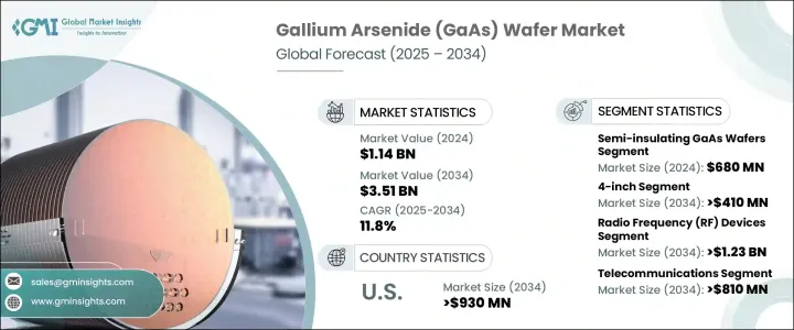
The Global Gallium Arsenide Wafer Market was valued at USD 1.14 billion in 2024 and is estimated to grow at a CAGR of 11.8% to reach USD 3.51 billion by 2034. The growth is largely attributed to the widespread adoption of 5G technology and advancements in photonics and optoelectronic devices. Gallium arsenide offers advantages over traditional materials like silicon due to its higher electron mobility and saturation velocity, making it suitable for high-frequency and high-speed applications. As the rollout of 5G infrastructure accelerates globally, the demand for RF components built using GaAs wafers has risen sharply.
These wafers are essential for developing components that power next-gen wireless systems by supporting faster data transfer rates and lower latency. Apart from telecommunications, GaAs wafers are heavily utilized in optoelectronic applications due to their direct bandgap, which supports efficient light emission and detection. The ongoing development in communication networks, along with expanding uses in laser technologies and photodetectors, is significantly strengthening the growth trajectory of the GaAs wafer market across major economies. Increasing focus on high-performance electronics and secure supply chains is also supporting the adoption of these wafers in strategic sectors.
| Market Scope | |
|---|---|
| Start Year | 2024 |
| Forecast Year | 2025-2034 |
| Start Value | $1.14 Billion |
| Forecast Value | $3.51 Billion |
| CAGR | 11.8% |
The Asia-Pacific region is emerging as a hub for GaAs wafer production, with several countries investing heavily in next-generation telecom infrastructure, boosting demand for RF components. North America is also witnessing considerable momentum, driven by rapid 5G adoption and an increasing need for advanced wireless systems. The region's growing reliance on GaAs wafers to enhance high-frequency capabilities highlights their strategic importance in modern communications. The material's effectiveness in handling large data streams with minimal delay is making it increasingly essential to next-gen technologies. Meanwhile, the global optoelectronics sector continues to integrate gallium arsenide into devices like LEDs, laser emitters, and light sensors, leveraging its superior electron mobility and bandgap structure.
Semi-insulating GaAs wafers, valued at USD 680 million in 2024, lead the market segment because they are essential in building RF and microwave components. Their low carrier concentration and high resistivity make them perfect for fabricating RF switches and amplifiers, which are widely used across various high-frequency communication platforms. Their ability to minimize signal interference makes them a top choice in environments demanding precision and performance.
The 4-inch GaAs wafer segment is forecast to reach USD 410 million by 2034. These wafers remain the most preferred in manufacturing, largely because of their established compatibility with production equipment and high usage volumes in RF and optoelectronic components. Their longstanding presence in the market ensures a steady supply chain and ease of integration into commercial-scale operations, making them a standard for many applications.
United States Gallium Arsenide (GaAs) Wafer Market is poised to reach USD 930 million by 2034, fueled by growing demand from defense, aerospace, and wireless communication fields. Public and private investments in enhancing GaAs-based technologies are accelerating as the country prioritizes semiconductor independence and technological leadership. Increasing adoption in applications like LIDAR and satellite communication is further pushing the demand for GaAs wafers. Supportive policies and dedicated research are driving innovation and advancing domestic production capabilities in the region.
Key players actively shaping the Gallium Arsenide (GaAs) Wafer Market include WIN Semiconductors Corp., IQE plc, Sumitomo Electric Industries, Ltd., VPEC Inc. (Visual Photonics Epitaxy Company), and Toshiba Corporation. Prominent players in the GaAs wafer market are deploying a variety of strategic approaches to maintain a competitive edge and expand their global reach. They are consistently investing in R&D to improve wafer quality, increase production efficiency, and enhance device performance. Strategic collaborations with end-use industries are helping companies better align their offerings with evolving application needs. Many manufacturers are also focusing on capacity expansion and establishing regional manufacturing hubs to support local demand while minimizing supply chain risks. In addition, firms are strengthening their intellectual property portfolios and advancing proprietary epitaxy technologies to ensure product differentiation.
Table of Contents
Chapter 1 Methodology and Scope
- 1.1 Market scope and definitions
- 1.2 Research design
- 1.2.1 Research approach
- 1.2.2 Data collection methods
- 1.3 Base estimates and calculations
- 1.3.1 Base year calculation
- 1.3.2 Key trends for market estimation
- 1.4 Forecast model
- 1.5 Primary research and validation
- 1.5.1 Primary sources
- 1.5.2 Data mining sources
Chapter 2 Executive Summary
- 2.1 Industry 3600 synopsis
Chapter 3 Industry Insights
- 3.1 Industry ecosystem analysis
- 3.2 Trump administration tariffs
- 3.2.1 Impact on trade
- 3.2.1.1 Trade volume disruptions
- 3.2.1.2 Retaliatory measures
- 3.2.2 Impact on the industry
- 3.2.2.1 Supply-side impact (raw materials)
- 3.2.2.1.1 Price volatility in key materials
- 3.2.2.1.2 Supply chain restructuring
- 3.2.2.1.3 Production cost implications
- 3.2.2.2 Demand-side impact (selling price)
- 3.2.2.2.1 Price transmission to end markets
- 3.2.2.2.2 Market share dynamics
- 3.2.2.2.3 Consumer response patterns
- 3.2.2.1 Supply-side impact (raw materials)
- 3.2.3 Key companies impacted
- 3.2.4 Strategic industry responses
- 3.2.4.1 Supply chain reconfiguration
- 3.2.4.2 Pricing and product strategies
- 3.2.4.3 Policy engagement
- 3.2.5 Outlook and future considerations
- 3.2.1 Impact on trade
- 3.3 Vendor matrix
- 3.4 Profit margin analysis
- 3.5 Technology & innovation landscape
- 3.6 Patent analysis
- 3.7 Key news and initiatives
- 3.8 Industry impact forces
- 3.8.1 Growth drivers
- 3.8.1.1 Rising demand for high-frequency RF devices
- 3.8.1.2 Expansion of optoelectronics applications
- 3.8.1.3 Growth in ADAS and autonomous vehicles
- 3.8.1.4 Adoption in space and military communications
- 3.8.1.5 Transition to larger wafer sizes (6-inch)
- 3.8.2 Industry pitfalls and challenges
- 3.8.2.1 High manufacturing costs and complex fabrication
- 3.8.2.2 Silicon and SiGe technology advancements
- 3.8.1 Growth drivers
- 3.9 Growth potential analysis
- 3.10 Regulatory landscape
- 3.11 Technology landscape
- 3.12 Future market trends
- 3.13 Gap analysis
- 3.14 Porter's analysis
- 3.15 PESTEL analysis
Chapter 4 Competitive Landscape, 2024
- 4.1 Introduction
- 4.2 Company market share analysis
- 4.3 Competitive analysis of major market players
- 4.4 Competitive positioning matrix
- 4.5 Strategy dashboard
Chapter 5 Market Estimates & Forecast, By Wafer Type, 2021 - 2034 (USD Million)
- 5.1 Semi-insulating GaAs wafers
- 5.2 Semi-conducting GaAs wafers
Chapter 6 Market estimates & forecast, By Wafer Size, 2021 - 2034 (USD Million)
- 6.1 2-inch
- 6.2 4-inch
- 6.3 6-inch
- 6.4 8-inch
Chapter 7 Market Estimates & Forecast, By Application, 2021 - 2034 (USD Million)
- 7.1 Radio frequency (RF) devices
- 7.2 Optoelectronic devices
- 7.3 Photovoltaic devices
- 7.4 Monolithic microwave integrated circuits (MMICs)
Chapter 8 Market estimates & forecast, By End Use, 2021 - 2034 (USD Million)
- 8.1 Telecommunications
- 8.2 Consumer electronics
- 8.3 Automotive
- 8.4 Aerospace & defense
- 8.5 Industrial automation
- 8.6 Energy & power
- 8.7 Others
Chapter 9 Market Estimates and Forecast, By Region, 2021 - 2034 (USD Million)
- 9.1 Key trends
- 9.2 North America
- 9.2.1 U.S.
- 9.2.2 Canada
- 9.3 Europe
- 9.3.1 Germany
- 9.3.2 UK
- 9.3.3 France
- 9.3.4 Spain
- 9.3.5 Italy
- 9.3.6 Netherlands
- 9.4 Asia Pacific
- 9.4.1 China
- 9.4.2 India
- 9.4.3 Japan
- 9.4.4 Australia
- 9.4.5 South Korea
- 9.5 Latin America
- 9.5.1 Brazil
- 9.5.2 Mexico
- 9.5.3 Argentina
- 9.6 Middle East and Africa
- 9.6.1 Saudi Arabia
- 9.6.2 South Africa
- 9.6.3 UAE
Chapter 10 Company Profiles
- 10.1 Analog Devices Inc.
- 10.2 AWSC (Advanced Wireless Semiconductor Company)
- 10.3 AXT Inc.
- 10.4 Broadcom Inc.
- 10.5 Coherent Corp.
- 10.6 Cree (Wolfspeed)
- 10.7 Freiberger Compound Materials GmbH
- 10.8 Fujitsu Semiconductor Limited
- 10.9 IntelliEPI Inc.
- 10.10 IQE plc
- 10.11 MACOM Technology Solutions
- 10.12 Northrop Grumman Corporation
- 10.13 Qorvo Inc.
- 10.14 RFHIC Corporation
- 10.15 Skyworks Solutions Inc.
- 10.16 Sumitomo Electric Industries, Ltd.
- 10.17 Toshiba Corporation
- 10.18 VPEC Inc.
- 10.19 WIN Semiconductors Corp.

