
PUBLISHER: Global Market Insights Inc. | PRODUCT CODE: 1871100

PUBLISHER: Global Market Insights Inc. | PRODUCT CODE: 1871100
Photoresist Chemicals for Advanced Lithography Market Opportunity, Growth Drivers, Industry Trend Analysis, and Forecast 2025 - 2034
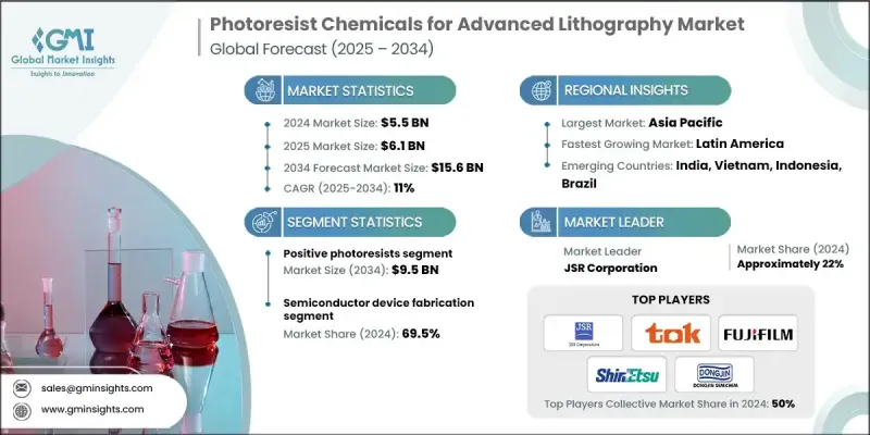
The Global Photoresist Chemicals for Advanced Lithography Market was valued at USD 5.5 Billion in 2024 and is estimated to grow at a CAGR of 11% to reach USD 15.6 Billion by 2034.
The market is being propelled by rising investments in the Asia-Pacific region, the commercialization of High-NA EUV systems, and advancements in 3D packaging technologies. The adoption of sub-7nm and sub-5nm process nodes, growing use of EUV lithography, and increasing demand for high-performance chips in AI, 5G, and automotive applications are driving this transformation. Extreme Ultraviolet (EUV) lithography at 13.5 nm wavelengths is enabling the patterning of 5nm line widths, significantly boosting demand for chemically amplified resists (CARs) and metal-oxide-based EUV photoresists. The evolution toward High-NA EUV, hybrid lithography combining DUV and EUV, and directed self-assembly (DSA) is reshaping resist chemistries. Industry leaders like JSR, TOK, Dongjin Semichem, and Fujifilm are aligning product roadmaps with 2nm and 1.4nm node readiness, marking a clear shift from traditional KrF/i-line resists to EUV-focused platforms.
| Market Scope | |
|---|---|
| Start Year | 2024 |
| Forecast Year | 2025-2034 |
| Start Value | $5.5 Billion |
| Forecast Value | $15.6 Billion |
| CAGR | 11% |
The positive photoresists segment generated USD 3.4 Billion in 2024 and is expected to reach USD 9.5 Billion by 2034, growing at a CAGR of 10.7%. Chemically amplified resists dominate this segment, offering high sensitivity for sub-10nm geometries and enabling precise process control. Innovations in this space focus on improving etch resistance, developing modular photoresist options, and minimizing secondary electron blur in EUV lithography, all critical to maximizing yields at small dimensions.
The semiconductor device fabrication segment held a 69.5% share in 2024 owing to its need for high-purity, high-performance photoresists used in advanced logic, memory, analog, and AI-focused chips. Increasing multi-patterning complexity and High-NA EUV adoption make logic devices, including CPUs, GPUs, and SoCs produced at 5nm, 3nm, and soon 2nm nodes, the largest consumers of photoresist materials.
U.S. Photoresist Chemicals for Advanced Lithography Market generated USD 817.4 million in 2024 and is expected to grow at a CAGR of 10.8% to reach USD 2.3 Billion by 2034. North America's growth is being fueled by semiconductor revitalization policies, including legislation encouraging domestic chip production. These policies are driving the demand for locally sourced photoresist and advanced lithography materials as new fabrication facilities are established by major manufacturers.
Key players in the Photoresist Chemicals for Advanced Lithography Market include Merck KGaA, Brewer Science, Inc., Dow, Fujifilm Holdings Corporation, Inpria Corporation, Dongjin Semichem Co., Ltd., Eternal Materials Co., Ltd., Shin-Etsu Chemical Co., Ltd., JSR Corporation, Kayaku Advanced Materials, Tokyo Ohka Kogyo Co., Ltd., Micro Resist Technology GmbH, Sumitomo Chemical Company, Jiangsu Nata Opto-electronic Material Co., Ltd., and Irresistible Materials Ltd. Leading companies are investing heavily in R&D to develop next-generation resist chemistries suitable for High-NA EUV and sub-5nm process nodes. Strategic collaborations with semiconductor manufacturers help align product innovations with commercial lithography requirements. Firms are expanding production capacities in Asia-Pacific and North America to meet rising regional demand. Some players focus on hybrid lithography solutions and directed self-assembly technologies to broaden product applicability.
Table of Contents
Chapter 1 Methodology & Scope
- 1.1 Market scope and definition
- 1.2 Research design
- 1.2.1 Research approach
- 1.2.2 Data collection methods
- 1.3 Data mining sources
- 1.3.1 Global
- 1.3.2 Regional/Country
- 1.4 Base estimates and calculations
- 1.4.1 Base year calculation
- 1.4.2 Key trends for market estimation
- 1.5 Primary research and validation
- 1.5.1 Primary sources
- 1.6 Forecast model
- 1.7 Research assumptions and limitations
Chapter 2 Executive Summary
- 2.1 Industry 360° synopsis
- 2.2 Key market trends
- 2.2.1 Regional
- 2.2.2 Type
- 2.2.3 Lithography technology
- 2.2.4 End use
- 2.3 TAM Analysis, 2025-2034
- 2.4 CXO perspectives: Strategic imperatives
- 2.4.1 Executive decision points
- 2.4.2 Critical success factors
- 2.5 Future Outlook and Strategic Recommendations
Chapter 3 Industry Insights
- 3.1 Industry ecosystem analysis
- 3.1.1 Supplier Landscape
- 3.1.2 Profit Margin
- 3.1.3 Value addition at each stage
- 3.1.4 Factor affecting the value chain
- 3.1.5 Disruptions
- 3.2 Industry impact forces
- 3.2.1 Growth drivers
- 3.2.2 Industry pitfalls and challenges
- 3.2.3 Market opportunities
- 3.3 Growth potential analysis
- 3.4 Regulatory landscape
- 3.4.1 North America
- 3.4.2 Europe
- 3.4.3 Asia Pacific
- 3.4.4 Latin America
- 3.4.5 Middle East & Africa
- 3.5 Porter's analysis
- 3.6 PESTEL analysis
- 3.7 Price trends
- 3.7.1 By region
- 3.7.2 By type
- 3.8 Future market trends
- 3.9 Technology and Innovation landscape
- 3.9.1 Current technological trends
- 3.9.2 Emerging technologies
- 3.10 Patent Landscape
- 3.11 Trade statistics ( Note: the trade statistics will be provided for key countries only)
- 3.11.1 Major importing countries
- 3.11.2 Major exporting countries
- 3.12 Sustainability and Environmental Aspects
- 3.12.1 Sustainable Practices
- 3.12.2 Waste Reduction Strategies
- 3.12.3 Energy Efficiency in Production
- 3.12.4 Eco-friendly Initiatives
- 3.13 Carbon Footprint Considerations
Chapter 4 Competitive Landscape, 2024
- 4.1 Introduction
- 4.2 Company market share analysis
- 4.2.1 By region
- 4.2.1.1 North America
- 4.2.1.2 Europe
- 4.2.1.3 Asia Pacific
- 4.2.1.4 LATAM
- 4.2.1.5 MEA
- 4.2.1 By region
- 4.3 Company matrix analysis
- 4.4 Competitive analysis of major market players
- 4.5 Competitive positioning matrix
- 4.6 Key developments
- 4.6.1 Mergers & acquisitions
- 4.6.2 Partnerships & collaborations
- 4.6.3 New Product Launches
- 4.7 Expansion Plans
Chapter 5 Market Estimates and Forecast, By Type, 2021 - 2034 (USD Million) (Tons)
- 5.1 Key trends
- 5.2 Positive photoresists
- 5.2.1 Acrylate-based photoresists
- 5.2.2 Novolac-based (dnq) systems
- 5.2.3 Poly (methyl methacrylate) (PMMA)
- 5.3 Negative photoresists
- 5.3.1 Epoxy-based
- 5.3.2 Silicon-containing resists
- 5.3.3 Metal-based resists
Chapter 6 Market Estimates and Forecast, By Lithography Technology, 2021 - 2034 (USD Million) (Tons)
- 6.1 Key trends
- 6.2 Duv lithography
- 6.2.1 248nm krf lithography
- 6.2.2 193nm dry lithography
- 6.2.3 193nm immersion lithography (arfi)
- 6.3 Extreme ultraviolet (euv) lithography
- 6.3.1 Euv @ 13.5 nm
- 6.3.2 High-na euv
- 6.4 I-line lithography (365 nm)
- 6.5 Nanoimprint lithography (nil)
- 6.6 E-beam lithography
Chapter 7 Market Estimates and Forecast, By End Use, 2021 - 2034 (USD Million) (Tons)
- 7.1 Key trends
- 7.2 Semiconductor device fabrication
- 7.2.1 Logic devices
- 7.2.2 Memory devices
- 7.2.3 Edge devices
- 7.2.4 Image sensors
- 7.3 Mems devices
- 7.3.1 Automotive mems
- 7.3.2 Consumer electronics mems
- 7.3.3 Industrial & healthcare mems
- 7.4 Display electronics applications
- 7.4.1 LCD manufacturing
- 7.4.2 OLED display production
- 7.4.3 Next-generation displays
- 7.5 Advanced packaging applications
- 7.5.1 3d packaging
- 7.5.2 System-in-package (SIP)
- 7.5.3 Wafer-level packaging (WLP)
- 7.6 Photomask manufacturing
- 7.6.1 EUV mask
- 7.6.2 DUV mask
Chapter 8 Market Estimates and Forecast, By Region, 2021 - 2034 (USD Million) (Tons)
- 8.1 Key trends
- 8.2 North America
- 8.2.1 U.S.
- 8.2.2 Canada
- 8.3 Europe
- 8.3.1 Germany
- 8.3.2 UK
- 8.3.3 France
- 8.3.4 Spain
- 8.3.5 Italy
- 8.3.6 Rest of Europe
- 8.4 Asia Pacific
- 8.4.1 China
- 8.4.2 India
- 8.4.3 Japan
- 8.4.4 Australia
- 8.4.5 South Korea
- 8.4.6 Rest of Asia Pacific
- 8.5 Latin America
- 8.5.1 Brazil
- 8.5.2 Mexico
- 8.5.3 Argentina
- 8.5.4 Rest of Latin America
- 8.6 Middle East and Africa
- 8.6.1 Saudi Arabia
- 8.6.2 South Africa
- 8.6.3 UAE
- 8.6.4 Rest of Middle East and Africa
Chapter 9 Company Profiles
- 9.1 Brewer Science, Inc.
- 9.2 Dongjin Semichem Co., Ltd.
- 9.3 Dow
- 9.4 Eternal Materials Co., Ltd.
- 9.5 Fujifilm Holdings Corporation
- 9.6 Inpria Corporation
- 9.7 Irresistible Materials Ltd.
- 9.8 Jiangsu Nata Opto-electronic Material Co., Ltd.
- 9.9 JSR Corporation
- 9.10 Kayaku Advanced Materials
- 9.11 Merck KGaA
- 9.12 Micro Resist Technology GmbH
- 9.13 Shin-Etsu Chemical Co., Ltd.
- 9.14 Sumitomo Chemical Company
- 9.15 Tokyo Ohka Kogyo Co., Ltd.
- 9.16 Others

