
PUBLISHER: Global Market Insights Inc. | PRODUCT CODE: 1913281

PUBLISHER: Global Market Insights Inc. | PRODUCT CODE: 1913281
Through-Silicon Via (TSV) Technology Market Opportunity, Growth Drivers, Industry Trend Analysis, and Forecast 2026 - 2035
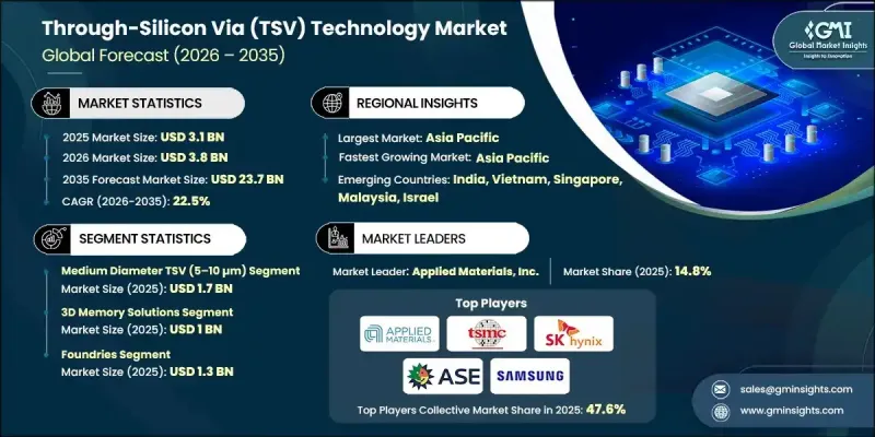
The Global Through-Silicon Via (TSV) Technology Market was valued at USD 3.1 billion in 2025 and is estimated to grow at a CAGR of 22.5% to reach USD 23.7 billion by 2035.
Rising demand for compact, power-efficient semiconductor solutions continues to reshape chip design strategies worldwide. Increased deployment of advanced wireless networks places greater performance expectations on edge devices and mobile platforms, driving the need for smaller footprints and higher bandwidth efficiency. TSV technology enables vertical integration that reduces form factor size while improving electrical performance. Manufacturers increasingly shift away from conventional planar scaling as economic and technical limitations emerge at smaller nodes. Three-dimensional architectures and chiplet-based designs gain traction as viable pathways to sustain performance gains. Since the late 1990s, the adoption of stacked memory and sensor architectures steadily accelerated. By the early 2020s, most integrated device manufacturers incorporate TSV-enabled three-dimensional designs into long-term performance planning. Toward the next decade, vertical stacking becomes a primary driver of advancement for processors and accelerators. At the same time, regionalized semiconductor production and automation-driven manufacturing reshape TSV supply chains. Early process limitations related to copper filling, wafer thinning, and planarization variability drive continuous improvement efforts across fabrication workflows.
| Market Scope | |
|---|---|
| Start Year | 2025 |
| Forecast Year | 2026-2035 |
| Start Value | $3.1 Billion |
| Forecast Value | $23.7 Billion |
| CAGR | 22.5% |
The medium diameter TSVs, ranging from 5 to 10 micrometers, represent the largest segment and generated USD 1.7 billion in 2025. Growing requirements for miniaturization, thermal efficiency, and reliable power delivery encourage broader adoption of advanced three-dimensional packaging solutions. Manufacturers in this segment focus on achieving precision manufacturing, thermal stability, energy efficiency, and scalable cost structures to support rising volumes of high-density semiconductor devices.
The three-dimensional memory solutions segment generated USD 1 billion in 2025. Commercial availability of next-generation high-bandwidth memory accelerates the use of TSV-enabled stacked memory architectures. Demand from large-scale computing environments increases the need for vertically integrated memory with fast interconnect performance, reinforcing the importance of TSV-based designs for low-latency data processing.
U.S. Through-Silicon Via (TSV) Technology Market reached USD 512 million in 2025 and is projected to grow at a CAGR of 22.3% from 2026 to 2035. Federal funding of USD 52.7 billion supports domestic fabrication, outsourced semiconductor assembly and testing, and advanced packaging initiatives. This investment strengthens TSV adoption across memory, processors, and artificial intelligence accelerators while supporting national supply chain resilience. Expanding use of chiplets and high-density computing in data centers further drives demand, encouraging manufacturers to align infrastructure investments with domestic foundries and cloud service providers.
Key companies active in the Global Through-Silicon Via (TSV) Technology Market include Taiwan Semiconductor Manufacturing Company Limited, Intel Corporation, Applied Materials, Inc., Samsung, ASE Group, Lam Research, Amkor Technology, SK Hynix, Toshiba Corporation, Powertech Technology, Okmetic Oyj, Teledyne DALSA, Atomica Corp, Japan Semiconductor Corporation, Nanosystems JP, and imec. Companies operating in the Global Through-Silicon Via (TSV) Technology Market strengthen their competitive position through sustained investment in advanced packaging research, process automation, and yield optimization. Strategic collaboration across foundries, OSATs, and system designers supports faster adoption of three-dimensional integration. Many players focus on co-development frameworks to align TSV architectures with next-generation processors and memory platforms. Expanding localized manufacturing capacity improves supply chain security and reduces production risk. Firms also emphasize scalable process technologies that lower the cost per interconnect while improving reliability.
Table of Contents
Chapter 1 Methodology & Scope
- 1.1 Market scope and definition
- 1.2 Research design
- 1.2.1 Research approach
- 1.2.2 Data collection methods
- 1.3 Data mining sources
- 1.3.1 Global
- 1.3.2 Regional/Country
- 1.4 Base estimates and calculations
- 1.4.1 Base year calculation
- 1.4.2 Key trends for market estimation
- 1.5 Primary research and validation
- 1.5.1 Primary sources
- 1.6 Forecast model
- 1.7 Research assumptions and limitations
Chapter 2 Executive Summary
- 2.1 Industry 360° synopsis
- 2.2 Key market trends
- 2.2.1 TSV process trends
- 2.2.2 TSV diameter trends
- 2.2.3 Application trends
- 2.2.4 End-use industry trends
- 2.2.5 Regional trends
- 2.3 TAM Analysis, 2026-2035 (USD Billion)
- 2.4 CXO perspectives: Strategic imperatives
- 2.4.1 Executive decision points
- 2.4.2 Critical Success Factors
- 2.5 Future Outlook and Strategic Recommendations
Chapter 3 Industry Insights
- 3.1 Industry ecosystem analysis
- 3.1.1 Factor affecting the value chain
- 3.1.2 Profit margin analysis
- 3.1.3 Disruptions
- 3.1.4 Future outlook
- 3.1.5 Manufacturers
- 3.1.6 Distributors
- 3.2 Impact forces
- 3.2.1 Growth drivers
- 3.2.1.1 Mobile & 5G / edge devices needing miniaturization
- 3.2.1.2 Regional fabs and government support
- 3.2.1.3 AI / HPC demand for bandwidth & density
- 3.2.1.4 Heterogeneous integration (chiplets, 2.5D/3D ICs)
- 3.2.1.5 Manufacturing ecosystem maturation & equipment investment
- 3.2.2 Industry pitfalls & challenges
- 3.2.2.1 Manufacturing cost, process complexity & yield loss
- 3.2.2.2 Thermo-mechanical reliability (CTE mismatch & stress)
- 3.2.3 Opportunities
- 3.2.3.1 High-Performance Computing (HPC) & AI
- 3.2.3.2 3D Stacked Memory Integration
- 3.2.1 Growth drivers
- 3.3 Growth potential analysis
- 3.4 Regulatory landscape
- 3.4.1 North America
- 3.4.2 Europe
- 3.4.3 Asia Pacific
- 3.4.4 Latin America
- 3.4.5 Middle East & Africa
- 3.5 Porter's analysis
- 3.6 PESTEL analysis
- 3.7 Technology and Innovation landscape
- 3.7.1 Current technological trends
- 3.7.2 Emerging technologies
- 3.8 Emerging Business Models
- 3.9 Compliance Requirements
- 3.10 Sustainability Measures
- 3.11 Consumer Sentiment Analysis
- 3.12 Patent and IP analysis
- 3.13 Geopolitical and trade dynamics
Chapter 4 Competitive Landscape, 2025
- 4.1 Introduction
- 4.2 Company market share analysis
- 4.2.1 By region
- 4.2.1.1 North America
- 4.2.1.2 Europe
- 4.2.1.3 Asia Pacific
- 4.2.1.4 Latin America
- 4.2.1.5 Middle East & Africa
- 4.2.2 Market Concentration Analysis
- 4.2.1 By region
- 4.3 Competitive Benchmarking of key Players
- 4.3.1 Financial Performance Comparison
- 4.3.1.1 Revenue
- 4.3.1.2 Profit Margin
- 4.3.1.3 R&D
- 4.3.2 Product Portfolio Comparison
- 4.3.2.1 Product Range Breadth
- 4.3.2.2 Technology
- 4.3.2.3 Innovation
- 4.3.3 Geographic Presence Comparison
- 4.3.3.1 Global Footprint Analysis
- 4.3.3.2 Service Network Coverage
- 4.3.3.3 Market Penetration by Region
- 4.3.4 Competitive Positioning Matrix
- 4.3.4.1 Leaders
- 4.3.4.2 Challengers
- 4.3.4.3 Followers
- 4.3.4.4 Niche Players
- 4.3.5 Strategic outlook matrix
- 4.3.1 Financial Performance Comparison
- 4.4 Key developments, 2022-2025
- 4.4.1 Mergers and Acquisitions
- 4.4.2 Partnerships and Collaborations
- 4.4.3 Technological Advancements
- 4.4.4 Expansion and Investment Strategies
- 4.4.5 Sustainability Initiatives
- 4.4.6 Digital Transformation Initiatives
- 4.5 Emerging/ Startup Competitors Landscape
Chapter 5 Market Estimates & Forecast, By TSV Process Type, 2022-2035 (USD Billion)
- 5.1 Key trends
- 5.2 Via-First TSV
- 5.3 Via-Middle TSV
- 5.4 Via-Last TSV
Chapter 6 Market Estimates & Forecast, By TSV Diameter, 2022-2035 (USD Billion)
- 6.1 Key trends
- 6.2 Large diameter TSV (>10 µm)
- 6.3 Medium diameter TSV (5-10 µm)
- 6.4 Small diameter TSV (<5 µm)
Chapter 7 Market Estimates & Forecast, By Application, 2022-2035 (USD Billion)
- 7.1 Key trends
- 7.2 3D memory solutions
- 7.2.1 High bandwidth memory (HBM)
- 7.2.2 Wide I/O memory
- 7.2.3 3D NAND flash memory
- 7.3 Processors & compute devices
- 7.3.1 CPUs
- 7.3.2 GPUs
- 7.3.3 AI Accelerators
- 7.3.4 FPGAs
- 7.4 CMOS image sensors
- 7.5 MEMS devices
- 7.5.1 Inertial sensors
- 7.5.2 Pressure sensors
- 7.5.3 Microphones
- 7.5.4 Others
- 7.6 RF & communication devices
- 7.7 Others
Chapter 8 Market Estimates & Forecast, By End Use Industry, 2022-2035 (USD Billion)
- 8.1 Key trends
- 8.2 Integrated device manufacturers (IDMs)
- 8.3 Foundries
- 8.4 OSATs (Outsourced semiconductor assembly & test)
- 8.5 Fabless semiconductor companies
- 8.6 Others
Chapter 9 Market Estimates & Forecast, By Region, 2022-2035 (USD Billion)
- 9.1 Key trends
- 9.2 North America
- 9.2.1 U.S.
- 9.2.2 Canada
- 9.3 Europe
- 9.3.1 UK
- 9.3.2 Germany
- 9.3.3 France
- 9.3.4 Italy
- 9.3.5 Spain
- 9.3.6 Russia
- 9.4 Asia Pacific
- 9.4.1 China
- 9.4.2 India
- 9.4.3 Japan
- 9.4.4 South Korea
- 9.4.5 Australia
- 9.5 Latin America
- 9.5.1 Brazil
- 9.5.2 Mexico
- 9.6 MEA
- 9.6.1 South Africa
- 9.6.2 Saudi Arabia
- 9.6.3 UAE
Chapter 10 Company Profiles
- 10.1 Global Key Players
- 10.1.1 Applied Materials, Inc.
- 10.1.2 Samsung
- 10.1.3 Taiwan Semiconductor Manufacturing Company Limited
- 10.1.4 SK Hynix
- 10.1.5 Intel Corporation
- 10.1.6 Lam Research
- 10.1.7 Toshiba Corporation
- 10.1.8 ASE Group
- 10.2 Regional Key Players
- 10.2.1 North America
- 10.2.1.1 Amkor Technology
- 10.2.1.2 Atomica Corp
- 10.2.2 Europe
- 10.2.2.1 Okmetic Oyj
- 10.2.2.2 Imec
- 10.2.3 Asia Pacific
- 10.2.4 Japan Semiconductor Corporation
- 10.2.5 Powertech Technology
- 10.2.1 North America
- 10.3 Niche Players/Disruptors
- 10.3.1 Teledyne DALSA
- 10.3.2 Nanosystems JP

