
PUBLISHER: Global Market Insights Inc. | PRODUCT CODE: 1959568

PUBLISHER: Global Market Insights Inc. | PRODUCT CODE: 1959568
E-Beam Wafer Inspection System Market Opportunity, Growth Drivers, Industry Trend Analysis, and Forecast 2026 - 2035
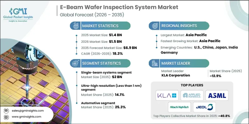
The Global E-Beam Wafer Inspection System Market was valued at USD 1.4 billion in 2025 and is estimated to grow at a CAGR of 18.3% to reach USD 6.9 billion by 2035.
The market's growth is fueled by rising investments in semiconductor manufacturing capacity and the increasing complexity of advanced devices. Manufacturers are integrating artificial intelligence (AI) and machine learning (ML) algorithms into inspection systems to improve defect detection and yield optimization. Demand is also driven by the proliferation of emerging technologies, including 5G, artificial intelligence, the Internet of Things (IoT), and automotive electronics, all of which require high-quality wafers. As wafer architectures become more intricate, the need for precise inspection tools has grown, particularly in consumer electronics, telecommunications, and memory fabrication industries.
| Market Scope | |
|---|---|
| Start Year | 2025 |
| Forecast Year | 2026-2035 |
| Start Value | $1.4 Billion |
| Forecast Value | $6.9 Billion |
| CAGR | 18.3% |
The adoption of advanced 3D device architectures, such as gate-all-around (GAA) transistors and 3D NAND, is creating significant challenges for defect characterization. Complex vertical structures and multilayer stacking exceed the capabilities of optical inspection systems, prompting manufacturers to rely increasingly on e-beam systems for logic and memory fabrication. E-beam inspection systems offer high-resolution imaging and accurate identification of structural defects, ensuring quality and reliability in advanced semiconductor manufacturing.
The single-beam systems segment is expected to reach USD 2 billion by 2035, driven by their affordability and suitability for research, development, and low- to mid-volume production. These systems provide high-resolution imaging with simpler deployment, making them ideal for small- to medium-scale fabs and academic research centers. Their ability to detect defects in sub-10 nm nodes supports yield learning and process optimization, reducing scrap and improving overall efficiency.
The ultra-high-resolution segment, defined by resolutions below 1 nm, held 14.1% share in 2025. Sub-nanometer imaging is critical for identifying patterning, stochastic, and material defects that lower-resolution systems cannot detect. This capability is essential for next-generation logic and memory devices, as well as EUV lithography processes, where even atomic-scale imperfections can significantly impact yield and device performance.
North America E-Beam Wafer Inspection System Market held a 33.2% share in 2025. The region's growth is supported by the presence of leading semiconductor manufacturers, advanced-node fabs, and early adoption of EUV lithography. High adoption of sub-7 nm processes, coupled with strong investments in R&D and advanced process control, makes e-beam inspection critical for defect detection and yield management. Collaborations between equipment vendors and fabs facilitate AI-driven defect analytics and multi-beam technologies, further reinforcing North America's market leadership.
Prominent players in the Global E-Beam Wafer Inspection System Market include Applied Materials, Inc., KLA Corporation, ASML Holding N.V., Hitachi High Technologies Corp., JEOL Ltd., Onto Innovation, Carl Zeiss SMT, Aerotech, Inc., MKS Inc., PDF Solutions, Thermo Fisher Scientific Inc., Camtek, Advantest Corporation, SCREEN SPE Tech Co., Ltd., and Wuhan Jingce Electronic Group. Companies in the Global E-Beam Wafer Inspection System Market are strengthening their foothold through strategic initiatives such as investing in AI and ML integration to enhance defect detection capabilities, expanding multi-beam system development for higher throughput, and forming partnerships with semiconductor fabs to customize solutions for advanced nodes. They are also focusing on global expansion to tap into emerging markets, enhancing service networks for predictive maintenance, and offering modular, scalable solutions for both high-volume manufacturing and R&D applications. Continuous innovation in sub-nanometer resolution, combined with software-driven process optimization, allows these companies to maintain competitiveness and reinforce long-term market leadership.
Table of Contents
Chapter 1 Methodology and Scope
- 1.1 Market scope and definition
- 1.2 Research design
- 1.2.1 Research approach
- 1.2.2 Data collection methods
- 1.3 Data mining sources
- 1.3.1 Global
- 1.3.2 Regional/Country
- 1.4 Base estimates and calculations
- 1.4.1 Base year calculation
- 1.4.2 Key trends for market estimation
- 1.5 Primary research and validation
- 1.5.1 Primary sources
- 1.6 Forecast model
- 1.7 Research assumptions and limitations
Chapter 2 Executive Summary
- 2.1 Industry 360° synopsis, 2022 - 2035
- 2.2 Key market trends
- 2.2.1 System type trends
- 2.2.2 Deployment model trends
- 2.2.3 End-user industry trends
- 2.2.4 Regional trends
- 2.3 TAM analysis, 2025-2035
- 2.4 CXO perspectives: Strategic imperatives
- 2.4.1 Executive decision points
- 2.4.2 Critical success factors
- 2.5 Future outlook and strategic recommendations
Chapter 3 Industry Insights
- 3.1 Industry ecosystem analysis
- 3.1.1 Supplier landscape
- 3.1.2 Profit margin analysis
- 3.1.3 Cost structure
- 3.1.4 Value addition at each stage
- 3.1.5 Factor affecting the value chain
- 3.1.6 Disruptions
- 3.2 Industry impact forces
- 3.2.1 Growth drivers
- 3.2.1.1 Escalating defect sensitivity requirements in advanced nodes
- 3.2.1.2 Expansion of semiconductor foundry capacity
- 3.2.1.3 Growing complexity of 3d device architectures
- 3.2.1.4 Rapid adoption of EUV lithography
- 3.2.1.5 Technological advancements in multi-beam e-beam systems
- 3.2.2 Industry pitfalls and challenges
- 3.2.2.1 Relatively low throughput compared to optical tools
- 3.2.2.2 Complexity of system integration into fab workflows
- 3.2.3 Market opportunities
- 3.2.3.1 Growth of subscription-based & mapping-as-a-service models
- 3.2.3.2 Expansion opportunities in underpenetrated markets
- 3.2.1 Growth drivers
- 3.3 Regulatory landscape
- 3.3.1 North America
- 3.3.2 Europe
- 3.3.3 Asia Pacific
- 3.3.4 Latin America
- 3.3.5 Middle East & Africa
- 3.4 Porter's analysis
- 3.5 PESTEL analysis
- 3.6 Technology and innovation landscape
- 3.6.1 Current technological trends
- 3.6.2 Emerging technologies
- 3.7 Emerging business models
- 3.8 Compliance requirements
- 3.9 Patent and IP analysis
- 3.10 Geopolitical and trade dynamics
Chapter 4 Competitive Landscape, 2025
- 4.1 Introduction
- 4.2 Company market share analysis
- 4.2.1 By region
- 4.2.1.1 North America
- 4.2.1.2 Europe
- 4.2.1.3 Asia Pacific
- 4.2.1.4 Latin America
- 4.2.1.5 Middle East & Africa
- 4.2.1 By region
- 4.3 Competitive benchmarking of key players
- 4.3.1 Financial performance comparison
- 4.3.1.1 Revenue
- 4.3.1.2 Profit margin
- 4.3.1.3 R&D
- 4.3.2 Product portfolio comparison
- 4.3.2.1 Product range breadth
- 4.3.2.2 Technology
- 4.3.2.3 Innovation
- 4.3.3 Geographic presence comparison
- 4.3.3.1 Global footprint analysis
- 4.3.3.2 Service network coverage
- 4.3.3.3 Market penetration by region
- 4.3.4 Competitive positioning matrix
- 4.3.4.1 Leaders
- 4.3.4.2 Challengers
- 4.3.4.3 Followers
- 4.3.4.4 Niche players
- 4.3.5 Strategic outlook matrix
- 4.3.1 Financial performance comparison
- 4.4 Key developments, 2022-2025
- 4.4.1 Mergers and acquisitions
- 4.4.2 Partnerships and collaborations
- 4.4.3 Technological advancements
- 4.4.4 Expansion and investment strategies
- 4.4.5 Digital transformation initiatives
- 4.5 Emerging/ startup competitors' landscape
Chapter 5 Market Estimates and Forecast, By System Architecture, 2022 - 2035 (USD Million, Units)
- 5.1 Key trends
- 5.2 Single-Beam Systems
- 5.3 Multi-Beam Systems
Chapter 6 Market Estimates and Forecast, By Resolution Capability, 2022 - 2035 (USD Million, Units)
- 6.1 Key trends
- 6.2 Ultra-High Resolution (Less than 1 nm)
- 6.3 High Resolution (1 nm to 10 nm)
- 6.4 Standard Resolution (More than 10 nm)
Chapter 7 Market Estimates and Forecast, By Process Stage, 2022 - 2035 (USD Million, Units)
- 7.1 Key trends
- 7.2 Front-End Wafer Inspection
- 7.3 Back-End Wafer Inspection
Chapter 8 Market Estimates and Forecast, By End-User Industry, 2022 - 2035 (USD Million, Units)
- 8.1 Key trends
- 8.2 Automotive
- 8.3 Consumer Electronics
- 8.4 Telecommunications
- 8.5 Industrial & Enterprise Electronics
- 8.6 Others
- 8.6.1 Healthcare / Medical Electronics
- 8.6.2 Defense / Aerospace Electronics
Chapter 9 Market Estimates and Forecast, By Region, 2022 - 2035 (USD Mn)
- 9.1 Key trends
- 9.2 North America
- 9.2.1 U.S.
- 9.2.2 Canada
- 9.3 Europe
- 9.3.1 Germany
- 9.3.2 UK
- 9.3.3 France
- 9.3.4 Spain
- 9.3.5 Italy
- 9.3.6 Netherlands
- 9.4 Asia Pacific
- 9.4.1 China
- 9.4.2 India
- 9.4.3 Japan
- 9.4.4 Australia
- 9.4.5 South Korea
- 9.5 Latin America
- 9.5.1 Brazil
- 9.5.2 Mexico
- 9.5.3 Argentina
- 9.6 Middle East and Africa
- 9.6.1 South Africa
- 9.6.2 Saudi Arabia
- 9.6.3 UAE
Chapter 10 Company Profiles
- 10.1 KLA Corporation
- 10.2 Applied Materials, Inc.
- 10.3 ASML Holding N.V.
- 10.4 Hitachi High Technologies Corp.
- 10.5 JEOL Ltd.
- 10.6 Onto Innovation.
- 10.7 Carl Zeiss SMT
- 10.8 Aerotech, Inc.
- 10.9 MKS Inc.
- 10.10 PDF Solutions
- 10.11 Wuhan Jingce Electronic Group
- 10.12 Thermo Fisher Scientific Inc.
- 10.13 Camtek
- 10.14 Advantest Corporation
- 10.15 SCREEN SPE Tech Co., Ltd.

