
PUBLISHER: Global Market Insights Inc. | PRODUCT CODE: 1982267

PUBLISHER: Global Market Insights Inc. | PRODUCT CODE: 1982267
Wafer Level Packaging Market Opportunity, Growth Drivers, Industry Trend Analysis, and Forecast 2026 - 2035
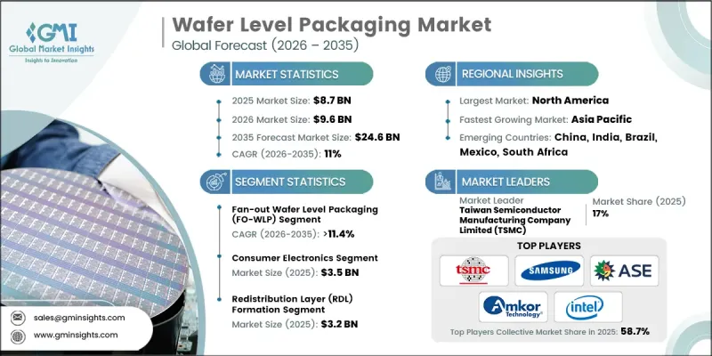
The Global Wafer Level Packaging Market was valued at USD 8.7 billion in 2025 and is estimated to grow at a CAGR of 11% to reach USD 24.6 billion by 2035.
Wafer level packaging is an advanced semiconductor manufacturing technique that completes the packaging process at the wafer stage before individual chip separation. This approach supports compact form factors, efficient thermal dissipation, and multi-die integration, enabling higher performance across advanced electronic systems. As industries push for greater computing capability, energy efficiency, and miniaturization, wafer level packaging is becoming a critical enabler of next-generation semiconductor innovation. The technology enhances interconnect density, improves signal integrity, and delivers cost advantages through streamlined production. Growing demand for high-performance and highly integrated semiconductor devices across data-driven, automotive, and connected ecosystems is accelerating adoption. Manufacturers are prioritizing scalable packaging architectures that address evolving design complexity while maintaining yield optimization and reliability standards. Overall, wafer level packaging continues to gain strategic importance within the global semiconductor value chain.
| Market Scope | |
|---|---|
| Start Year | 2025 |
| Forecast Year | 2026-2035 |
| Start Value | $8.7 Billion |
| Forecast Value | $24.6 Billion |
| CAGR | 11% |
Industries are rapidly adopting advanced semiconductor nodes to increase device performance and integration density. Wafer level packaging enables wafer-scale stacking and advanced interconnect solutions, supporting the development of high-reliability semiconductor products for emerging connectivity platforms, electrified mobility systems, and data-intensive infrastructure. Modern semiconductor applications require precise thermal management, enhanced yield performance, and dense interconnect architectures to meet complex integration demands. Wafer level packaging technologies support fan-out structures and panel-level scalability, enabling robust stacking solutions for three-dimensional integrated circuits and sensor modules used in advanced computing and intelligent systems. The integration of chiplet architectures, sophisticated redistribution layers, photonics compatibility, and AI-assisted assembly processes is further enhancing packaging efficiency.
The fan-out wafer level packaging segment was valued at USD 3.6 billion in 2025 and is estimated to grow at a CAGR of 11.4% during 2026-2035. This segment holds the largest share of the wafer level packaging market due to its ability to deliver higher input/output density, reduced interconnect length, and improved electrical and thermal performance. Its design adaptability and compatibility with heterogeneous integration architectures have strengthened its position in advanced semiconductor manufacturing. To address rising demand, manufacturers are focusing on durable, high-performance fan-out solutions supported by advanced redistribution layers, innovative molding materials, and scalable panel-level processing tools.
The redistribution layer formation segment generated USD 3.2 billion in 2025, leading the market by technology. This segment is expanding due to the increasing adoption of chiplet-based designs and three-dimensional heterogeneous integration in high-complexity semiconductor applications. Redistribution layer technology enables high-density interconnections between logic, memory, and power components, supporting advanced semiconductor functionality and enhanced system integration.
North America Wafer Level Packaging Market accounted for 42.6% share in 2025. Regional growth is driven by substantial semiconductor research and development activity, federal funding initiatives aimed at strengthening domestic fabrication capacity, and increasing demand for high-performance processors and advanced computing platforms. Leadership in packaging innovation and advanced semiconductor manufacturing continues to reinforce North America's dominant position within the global market.
Major companies operating in the Global Wafer Level Packaging Market include Taiwan Semiconductor Manufacturing Company Limited, Intel Corporation, Samsung Electronics Co., Ltd., ASE Technology Holding Co., Ltd., Amkor Technology, Inc., Jiangsu Changjiang Electronics Technology Co., Ltd., Powertech Technology Inc., Tongfu Microelectronics Co., Ltd., Huatian Technology Co., Ltd., ChipMOS Technologies Inc., China Wafer Level CSP Co., Ltd., HANA Micron Inc., STATS ChipPAC Pte. Ltd., Fujitsu Limited, and Deca Technologies Inc.. Companies competing in the Global Wafer Level Packaging Market are strengthening their competitive position through sustained investment in advanced packaging research and process innovation. Leading players are expanding panel-level manufacturing capabilities and developing next-generation redistribution layer technologies to improve integration density and thermal performance. Strategic collaborations with semiconductor foundries and system designers are enabling co-development of customized packaging architectures. Firms are also investing in automation, AI-driven inspection systems, and yield optimization tools to enhance production efficiency. Geographic expansion into emerging semiconductor hubs and capacity upgrades in advanced packaging facilities are supporting long-term growth.
Table of Contents
Chapter 1 Methodology and Scope
- 1.1 Market scope and definition
- 1.2 Research design
- 1.2.1 Research approach
- 1.2.2 Data collection methods
- 1.3 Data mining sources
- 1.3.1 Global
- 1.3.2 Regional/Country
- 1.4 Base estimates and calculations
- 1.4.1 Base year calculation
- 1.4.2 Key trends for market estimation
- 1.5 Primary research and validation
- 1.5.1 Primary sources
- 1.6 Forecast model
- 1.7 Research assumptions and limitations
Chapter 2 Executive Summary
- 2.1 Industry snapshot
- 2.2 Key market trends
- 2.2.1 Packaging type trends
- 2.2.2 Process trends
- 2.2.3 Material trends
- 2.2.4 End-use application trends
- 2.2.5 Regional trends
- 2.3 TAM Analysis, 2026-2035 (USD Billion)
- 2.4 CXO perspectives: Strategic imperatives
Chapter 3 Industry Insights
- 3.1 Industry ecosystem analysis
- 3.1.1 Supplier Landscape
- 3.1.2 Profit Margin
- 3.1.3 Cost structure
- 3.1.4 Value addition at each stage
- 3.1.5 Factor affecting the value chain
- 3.1.6 Disruptions
- 3.2 Industry impact forces
- 3.2.1 Growth drivers
- 3.2.1.1 Rising demand for miniaturization in mobile and wearables
- 3.2.1.2 Growth in AI accelerators and high-bandwidth memory
- 3.2.1.3 Expansion of automotive electronics and ADAS
- 3.2.1.4 Proliferation of 5G and edge computing devices
- 3.2.1.5 Increasing focus on cost reduction in high-volume production
- 3.2.2 Industry pitfalls and challenges
- 3.2.2.1 High equipment costs for panel-level WLP scaling
- 3.2.2.2 Technical challenges in yield for ultra-thin wafers
- 3.2.3 Market opportunities
- 3.2.3.1 Adoption of chiplet architectures and advanced SiPs
- 3.2.3.2 Growth in flexible/hybrid electronics and photonics
- 3.2.1 Growth drivers
- 3.3 Growth potential analysis
- 3.4 Regulatory landscape
- 3.4.1 North America
- 3.4.2 Europe
- 3.4.3 Asia Pacific
- 3.4.4 Latin America
- 3.4.5 Middle East & Africa
- 3.5 Porter's analysis
- 3.6 PESTEL analysis
- 3.7 Technology and innovation landscape
- 3.7.1 Current technological trends
- 3.7.2 Emerging technologies
- 3.8 Emerging business models
- 3.9 Compliance requirements
- 3.10 Patent analysis
Chapter 4 Competitive Landscape, 2025
- 4.1 Introduction
- 4.2 Company market share analysis
- 4.2.1 By Region
- 4.2.1.1 North America
- 4.2.1.2 Europe
- 4.2.1.3 Asia Pacific
- 4.2.1.4 Latin America
- 4.2.1.5 Middle East & Africa
- 4.2.2 Market Concentration Analysis
- 4.2.1 By Region
- 4.3 Competitive benchmarking of key players
- 4.3.1 Financial performance comparison
- 4.3.1.1 Revenue
- 4.3.1.2 Profit margin
- 4.3.1.3 R&D
- 4.3.2 Product portfolio comparison
- 4.3.2.1 Product range breadth
- 4.3.2.2 Technology
- 4.3.2.3 Innovation
- 4.3.3 Geographic presence comparison
- 4.3.3.1 Global footprint analysis
- 4.3.3.2 Service network coverage
- 4.3.3.3 Market penetration by region
- 4.3.4 Competitive positioning matrix
- 4.3.4.1 Leaders
- 4.3.4.2 Challengers
- 4.3.4.3 Followers
- 4.3.4.4 Niche players
- 4.3.5 Strategic outlook matrix
- 4.3.1 Financial performance comparison
- 4.4 Key developments, 2022-2025
- 4.4.1 Mergers and acquisitions
- 4.4.2 Partnerships and collaborations
- 4.4.3 Technological advancements
- 4.4.4 Expansion and investment strategies
- 4.4.5 Sustainability initiatives
- 4.4.6 Digital transformation initiatives
- 4.5 Emerging/ startup competitors landscape
Chapter 5 Market Estimates & Forecast, By Packaging Technology, 2022 - 2035 (USD Million)
- 5.1 Key trends,
- 5.2 Wafer-Level Chip Scale Packaging (WLCSP / WL-CSP)
- 5.3 Fan-In Wafer Level Packaging (FI-WLP)
- 5.4 Fan-Out Wafer Level Packaging (FO-WLP)
Chapter 6 Market Estimates and Forecast, By Process, 2022 - 2035 (USD Million)
- 6.1 Key trends
- 6.2 Redistribution Layer (RDL) formation
- 6.3 Wafer bumping
- 6.4 Wafer-level under-bump metallization (UBM)
- 6.5 Wafer-level passivation and protection layers
- 6.6 Wafer thinning and back grinding
Chapter 7 Market Estimates and Forecast, By Materials, 2022 - 2035 (USD Million)
- 7.1 Key trends
- 7.2 RDL materials
- 7.3 Dielectric and passivation materials
- 7.4 Solder and copper interconnect materials
- 7.5 Wafer-level encapsulation compounds
Chapter 8 Market Estimates and Forecast, By End-use Application, 2022 - 2035 (USD Million)
- 8.1 Key trends
- 8.2 Consumer electronics
- 8.3 Automotive electronics
- 8.4 Industrial electronics
- 8.5 IoT devices
- 8.6 Telecommunications devices
- 8.7 Others
Chapter 9 Wafer level packaging Market Estimates & Forecast, By Region, 2022 - 2035 (USD Million)
- 9.1 Key trends, by region
- 9.2 North America
- 9.2.1 U.S.
- 9.2.2 Canada
- 9.3 Europe
- 9.3.1 UK
- 9.3.2 Germany
- 9.3.3 France
- 9.3.4 Italy
- 9.3.5 Spain
- 9.3.6 Netherlands
- 9.3.7 Rest of Europe
- 9.4 Asia-Pacific
- 9.4.1 China
- 9.4.2 India
- 9.4.3 Japan
- 9.4.4 South Korea
- 9.4.5 Australia
- 9.4.6 Rest of Asia-Pacific
- 9.5 Latin America
- 9.5.1 Brazil
- 9.5.2 Mexico
- 9.5.3 Argentina
- 9.5.4 Rest of Latin America
- 9.6 MEA
- 9.6.1 Saudi Arabia
- 9.6.2 South Africa
- 9.6.3 UAE
- 9.6.4 Rest of MEA
Chapter 10 Company Profiles
- 10.1 Amkor Technology, Inc.
- 10.2 ASE Technology Holding Co., Ltd.
- 10.3 China Wafer Level CSP Co., Ltd.
- 10.4 ChipMOS Technologies Inc.
- 10.5 Deca Technologies Inc.
- 10.6 Fujitsu Limited
- 10.7 HANA Micron Inc.
- 10.8 Huatian Technology Co., Ltd.
- 10.9 Intel Corporation
- 10.10 Jiangsu Changjiang Electronics Technology Co., Ltd. (JCET Group)
- 10.11 Powertech Technology Inc. (PTI)
- 10.12 Samsung Electronics Co., Ltd.
- 10.13 STATS ChipPAC Pte. Ltd.
- 10.14 Taiwan Semiconductor Manufacturing Company Limited (TSMC)
- 10.15 Tongfu Microelectronics Co., Ltd.

