
PUBLISHER: Global Market Insights Inc. | PRODUCT CODE: 1982377

PUBLISHER: Global Market Insights Inc. | PRODUCT CODE: 1982377
Thin Wafer Market Opportunity, Growth Drivers, Industry Trend Analysis, and Forecast 2026 - 2035
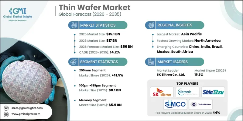
The Global Thin Wafer Market was valued at USD 15.1 billion in 2025 and is estimated to grow at a CAGR of 14.2% to reach USD 56 billion by 2035.
Thin wafers are semiconductor substrates processed through advanced back grinding, precision polishing, and chemical etching techniques to achieve a thickness of 200μm or below, typically ranging between 50μm and 100μm after front-side fabrication. These ultra-thin substrates are critical for next-generation power devices and compact electronic architectures, particularly in 3D stacking applications where high-density integration is required without exceeding 1μm total thickness variation. Their structural uniformity minimizes warping while enabling reliable handling during advanced packaging processes. Rising demand for miniaturized electronics, high-performance computing, and efficient power management solutions is accelerating adoption across multiple industries. Continuous advancements in semiconductor fabrication technologies and material engineering are further enhancing wafer durability, yield rates, and electrical performance, positioning thin wafers as a foundational component in modern semiconductor manufacturing.
| Market Scope | |
|---|---|
| Start Year | 2025 |
| Forecast Year | 2026-2035 |
| Start Value | $15.1 Billion |
| Forecast Value | $56 Billion |
| CAGR | 14.2% |
Growing electrification and automation within the automotive sector are significantly contributing to thin wafer demand. Increasing vehicle efficiency standards and emission reduction initiatives are driving the integration of advanced semiconductor components. Expanding electric vehicle adoption across emerging economies, along with investments in charging infrastructure and electronic control technologies, is reinforcing market expansion. In addition, public and private sector investments in semiconductor production, combined with rising research and development collaboration among leading players, are accelerating technological progress and manufacturing capacity growth.
The 125 mm/150 mm wafer size segment is expected to grow at a CAGR of 13.8% during 2026-2035. Rising automotive demand for compact and high-efficiency power integrated circuits and sensor solutions is fueling this segment. Broader deployment of connected devices, advanced communication infrastructure, and consumer electronics continues to support mature-node production processes utilizing smaller wafer formats for cost-effective manufacturing.
The 100μm-199μm thickness segment generated USD 8.1 billion in 2025. This segment maintains the largest share due to increasing utilization in power semiconductor applications supporting electric mobility and renewable energy systems. Thin wafers within this thickness range provide an optimal balance between mechanical integrity and electrical efficiency, supporting high-volume sensor manufacturing, power management integrated circuits, and advanced 3D packaging architectures. Manufacturers are emphasizing sophisticated temporary bonding solutions and carrier wafer technologies to improve process stability and performance outcomes in high-power semiconductor devices.
North America Thin Wafer Market accounted for 15.7% share in 2025. Regional growth is supported by the transition toward electrified automotive platforms, which require increased semiconductor content for advanced control and safety systems. Expansion in medical device manufacturing, demographic trends, and strategic semiconductor fabrication investments are contributing to sustained regional development through 2035.
Prominent companies operating in the Global Thin Wafer Market include SUMCO CORPORATION, Shin-Etsu Chemical Co., Ltd., Siltronic AG, GlobalWafers Co. Ltd., SK Siltron Co., Ltd., SOITEC, Applied Materials, Disco Corporation, EV Group, SUSS MicroTec, Okmetic, 3M, Brewer Science, Silicon Valley Microelectronics, Inc., UniversityWafer, Inc., Virginia Semiconductor Inc., Wafer Works Corporation, Shanghai Simgui Technology Co. Ltd., IceMOS Technology Ltd., Mechatronic Systemtechnik GmbH, Polishing Corporation of America, Sil'tronix Silicon Technologies, Skynova SA, Wafer World Inc., and WaferPro. Companies in the Global Thin Wafer Market are strengthening their competitive position through technological innovation, strategic alliances, and capacity expansion. Manufacturers are investing heavily in advanced material processing techniques, precision thinning equipment, and bonding technologies to enhance wafer uniformity and yield performance. Strategic collaborations with semiconductor foundries and device manufacturers enable early integration into next-generation chip designs. Firms are also expanding fabrication facilities to address rising global demand and improve supply chain resilience. Portfolio diversification into specialty substrates and engineered wafer solutions supports broader customer engagement.
Table of Contents
Chapter 1 Methodology and Scope
- 1.1 Market scope and definition
- 1.2 Research design
- 1.2.1 Research approach
- 1.2.2 Data collection methods
- 1.3 Data mining sources
- 1.3.1 Global
- 1.3.2 Regional/Country
- 1.4 Base estimates and calculations
- 1.4.1 Base year calculation
- 1.4.2 Key trends for market estimation
- 1.5 Primary research and validation
- 1.5.1 Primary sources
- 1.6 Forecast model
- 1.7 Research assumptions and limitations
Chapter 2 Executive Summary
- 2.1 Industry snapshot
- 2.2 Key market trends
- 2.2.1 Thickness trends
- 2.2.2 Wafer size trends
- 2.2.3 Process trends
- 2.2.4 Application trends
- 2.2.5 Regional trends
- 2.3 TAM Analysis, 2025-2034 (USD Billion)
- 2.4 CXO perspectives: Strategic imperatives
- 2.4.1 Executive decision points
- 2.4.2 critical success factors
- 2.5 Future outlook and strategic recommendations
Chapter 3 Industry Insights
- 3.1 Industry ecosystem analysis
- 3.1.1 Supplier Landscape
- 3.1.2 Profit Margin
- 3.1.3 Cost structure
- 3.1.4 Value addition at each stage
- 3.1.5 Factor affecting the value chain
- 3.1.6 Disruptions
- 3.2 Industry impact forces
- 3.2.1 Growth drivers
- 3.2.1.1 Advanced Semiconductor Packaging Demand
- 3.2.1.2 5G and AI Chip Proliferation
- 3.2.1.3 IoT Device Expansion
- 3.2.1.4 Electric Vehicle Power Electronics
- 3.2.1.5 CMOS Image Sensor Growth
- 3.2.2 Industry pitfalls and challenges
- 3.2.2.1 Wafer Warpage and Handling Challenges
- 3.2.2.2 High Defect Density and Yield Loss
- 3.2.3 Market opportunities
- 3.2.3.1 Advanced Packaging Innovation
- 3.2.3.2 Power Semiconductor Shift
- 3.2.1 Growth drivers
- 3.3 Growth potential analysis
- 3.4 Regulatory landscape
- 3.4.1 North America
- 3.4.2 Europe
- 3.4.3 Asia Pacific
- 3.4.4 Latin America
- 3.4.5 Middle East & Africa
- 3.5 Porter’s analysis
- 3.6 PESTEL analysis
- 3.7 Technology and innovation landscape
- 3.7.1 Current technological trends
- 3.7.2 Emerging technologies
- 3.8 Price trends
- 3.8.1 Historical price analysis (2022-2024)
- 3.8.2 Price trend drivers
- 3.8.3 Regional price variations
- 3.8.4 Price forecast (2026-2035)
- 3.9 Pricing strategies
- 3.10 Emerging business models
- 3.11 Compliance requirements
- 3.12 Patent analysis
Chapter 4 Competitive Landscape, 2025
- 4.1 Introduction
- 4.2 Company market share analysis
- 4.2.1 By Region
- 4.2.1.1 North America
- 4.2.1.2 Europe
- 4.2.1.3 Asia Pacific
- 4.2.1.4 Latin America
- 4.2.1.5 Middle East & Africa
- 4.2.2 Market Concentration Analysis
- 4.2.1 By Region
- 4.3 Competitive benchmarking of key players
- 4.3.1 Financial performance comparison
- 4.3.1.1 Revenue
- 4.3.1.2 Profit margin
- 4.3.1.3 R&D
- 4.3.2 Product portfolio comparison
- 4.3.2.1 Product range breadth
- 4.3.2.2 Technology
- 4.3.2.3 Innovation
- 4.3.3 Geographic presence comparison
- 4.3.3.1 Global footprint analysis
- 4.3.3.2 Service network coverage
- 4.3.3.3 Market penetration by region
- 4.3.4 Competitive positioning matrix
- 4.3.4.1 Leaders
- 4.3.4.2 Challengers
- 4.3.4.3 Followers
- 4.3.4.4 Niche players
- 4.3.5 Strategic outlook matrix
- 4.3.1 Financial performance comparison
- 4.4 Key developments, 2022-2025
- 4.4.1 Mergers and acquisitions
- 4.4.2 Partnerships and collaborations
- 4.4.3 Technological advancements
- 4.4.4 Expansion and investment strategies
- 4.4.5 Sustainability initiatives
- 4.4.6 Digital transformation initiatives
- 4.5 Emerging/ startup competitors landscape
Chapter 5 Market Estimates & Forecast, By Thickness, 2022 - 2035 (USD Million)
- 5.1 Key trends,
- 5.2 >200μm
- 5.3 100μm-199μm
- 5.4 50μm-99μm
- 5.5 30μm-49μm
- 5.6 10μm-29μm
- 5.7 <10μm
Chapter 6 Market Estimates and Forecast, By Wafer Size, 2022 - 2035 (USD Million)
- 6.1 Key trends
- 6.2 100 mm
- 6.3 125 mm/150mm
- 6.4 200 mm
- 6.5 300 mm
Chapter 7 Market Estimates and Forecast, By Process, 2022 - 2035 (USD Million)
- 7.1 Key trends
- 7.2 Temporary bonding & debonding
- 7.2.1 UV-release adhesives
- 7.2.2 Thermal-release adhesives
- 7.2.3 Solvent-release adhesives
- 7.3 Carrier-less approach/Taiko process
Chapter 8 Market Estimates and Forecast, By Application, 2022 - 2035 (USD Million)
- 8.1 Key trends
- 8.2 MEMS
- 8.3 CMOS image sensors
- 8.4 Memory
- 8.5 RF devices
- 8.6 LED
- 8.7 Interposers
- 8.8 Logic
- 8.9 Others
Chapter 9 Market Estimates & Forecast, By Region, 2022 - 2035 (USD Million)
- 9.1 Key trends, by region
- 9.2 North America
- 9.2.1 U.S.
- 9.2.2 Canada
- 9.3 Europe
- 9.3.1 UK
- 9.3.2 Germany
- 9.3.3 France
- 9.3.4 Italy
- 9.3.5 Spain
- 9.3.6 Netherlands
- 9.3.7 Rest of Europe
- 9.4 Asia-Pacific
- 9.4.1 China
- 9.4.2 India
- 9.4.3 Japan
- 9.4.4 South Korea
- 9.4.5 Australia
- 9.4.6 Rest of Asia-Pacific
- 9.5 Latin America
- 9.5.1 Brazil
- 9.5.2 Mexico
- 9.5.3 Argentina
- 9.5.4 Rest of Latin America
- 9.6 MEA
- 9.6.1 Saudi Arabia
- 9.6.2 South Africa
- 9.6.3 UAE
- 9.6.4 Rest of MEA
Chapter 10 Company Profiles
- 10.1 3M
- 10.2 Applied Materials
- 10.3 Brewer Science
- 10.4 Disco Corporation
- 10.5 EV Group
- 10.6 GlobalWafers Co. Ltd.
- 10.7 IceMOS Technology Ltd.
- 10.8 Mechatronic Systemtechnik GmbH
- 10.9 Okmetic
- 10.10 Polishing Corporation of America
- 10.11 Shanghai Simgui Technology Co. Ltd.
- 10.12 Shin-Etsu Chemical Co., Ltd.
- 10.13 Silicon Valley Microelectronics, Inc
- 10.14 Siltronic AG
- 10.15 Sil'tronix Silicon Technologies
- 10.16 SK Siltron Co., Ltd.
- 10.17 Skynova SA
- 10.18 SOITEC
- 10.19 SUMCO CORPORATION
- 10.20 SUSS MicroTec
- 10.21 UniversityWafer, Inc
- 10.22 Virginia Semiconductor Inc.
- 10.23 Wafer Works Corporation
- 10.24 Wafer World Inc.
- 10.25 WaferPro

