
PUBLISHER: Global Market Insights Inc. | PRODUCT CODE: 1982387

PUBLISHER: Global Market Insights Inc. | PRODUCT CODE: 1982387
SiC Wafer Reclaim Services Market Opportunity, Growth Drivers, Industry Trend Analysis, and Forecast 2026 - 2035
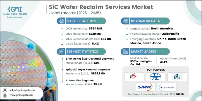
The Global SiC Wafer Reclaim Services Market was valued at USD 684 million in 2025 and is estimated to grow at a CAGR of 8.4% to reach USD 1.5 billion by 2035.
The growth is fueled by the rapid adoption of electric vehicles (EVs), which is increasing demand for silicon carbide-based power devices in applications like traction inverters, onboard chargers, and power management systems. These devices are preferred for their high efficiency, excellent thermal tolerance, and voltage handling capabilities. Government initiatives supporting semiconductor manufacturing, including incentives, subsidies, and fab expansion programs, are further driving demand for wafer reclaim services. Reclaiming wafers has become an essential cost-efficient manufacturing strategy, enabling higher yields and reduced material waste. There is a growing trend toward larger diameter wafers, particularly 150 mm and 200 mm, which requires advanced polishing, inspection, and surface characterization tools. Service providers are integrating sophisticated metrology and contamination control techniques to ensure high-quality reclaimed wafers that meet increasingly stringent flatness and defect tolerance requirements for automotive and industrial power electronics.
| Market Scope | |
|---|---|
| Start Year | 2025 |
| Forecast Year | 2026-2035 |
| Start Value | $684 Million |
| Forecast Value | $1.5 Billion |
| CAGR | 8.4% |
The above 10-inch (>250 mm) wafer segment is expected to grow at a CAGR of 8.9% during 2026-2035. Ultra-large wafers are critical for next-generation power devices, but processing them requires specialized equipment, precise layer removal, and advanced polishing techniques to avoid cracking, warping, or contamination. Manufacturers are refining these processes to minimize material loss, reduce production costs, and support large-scale deployment of SiC devices in automotive, industrial, and energy sectors.
The grinding & lapping services segment generated USD 168.1 million in 2025 and is anticipated to grow at a CAGR of 8.8% during 2026-2035. These services focus on achieving precise flatness, thickness, and surface smoothness for SiC wafers. Automation, process monitoring, and advanced abrasives are increasingly used to improve yields, minimize wafer-to-wafer variability, and enhance process consistency. Customized grinding and lapping solutions are being adopted to meet the requirements of high-power EV modules, industrial converters, and other specialized applications, enabling fabs to deliver reliable wafers while controlling costs.
North America SiC Wafer Reclaim Services Market held a 33.6% share in 2025. The region benefits from a well-established semiconductor ecosystem, strong automotive and industrial adoption of SiC devices, and advanced research infrastructure. A focus on clean energy initiatives further supports market growth across the U.S. and Canada.
Key players in the Global SiC Wafer Reclaim Services Market include Pure Wafer, Kinik Company, TOPCO Scientific, RS Technologies Co., Ltd., NOVA Electronic Materials, LLC, Scientech Corporation, Phoenix Silicon International Corporation, Semiconductor Industry Co., Ltd., and Mimasu. Companies in the Global SiC Wafer Reclaim Services Market are strengthening their positions by expanding their service capabilities, investing in advanced polishing and metrology technologies, and offering customized reclaim solutions for different wafer diameters and applications. Strategies include integrating automation and process monitoring to improve yields and reduce costs, developing proprietary methods for high-yield, low-defect wafer processing, and forming partnerships with semiconductor fabs to ensure a steady service pipeline. Firms are also exploring ultra-large wafer reclaim processes to meet the growing demand from automotive, industrial, and energy sectors, enhancing scalability and operational efficiency while maintaining high-quality standards.
Table of Contents
Chapter 1 Methodology and Scope
- 1.1 Market scope and definition
- 1.2 Research design
- 1.2.1 Research approach
- 1.2.2 Data collection methods
- 1.3 Data mining sources
- 1.3.1 Global
- 1.3.2 Regional/Country
- 1.4 Base estimates and calculations
- 1.4.1 Base year calculation
- 1.4.2 Key trends for market estimation
- 1.5 Primary research and validation
- 1.5.1 Primary sources
- 1.6 Forecast model
- 1.7 Research assumptions and limitations
Chapter 2 Executive Summary
- 2.1 Industry 360° synopsis, 2022 - 2035
- 2.2 Key market trends
- 2.2.1 Service type trends
- 2.2.2 Wafer diameter trends
- 2.2.3 Reclaim stage trends
- 2.2.4 End-use application trends
- 2.2.5 End-user trends
- 2.2.6 Regional trends
- 2.3 TAM analysis, 2025-2034
- 2.4 CXO perspectives: Strategic imperatives
- 2.4.1 Executive decision points
- 2.4.2 Critical success factors
Chapter 3 Industry Insights
- 3.1 Industry ecosystem analysis
- 3.1.1 Supplier landscape
- 3.1.2 Profit margin analysis
- 3.1.3 Cost structure
- 3.1.4 Value addition at each stage
- 3.1.5 Factor affecting the value chain
- 3.1.6 Disruptions
- 3.2 Industry impact forces
- 3.2.1 Growth drivers
- 3.2.1.1 Rising demand of SiC wafers in consumer electronics
- 3.2.1.2 Increasing adoption of semiconductors in solar energy
- 3.2.1.3 Growing penetration of SiC wafers for 5G and IoT devices
- 3.2.1.4 The increasing adoption of electric vehicles (EV)
- 3.2.1.5 Rising government initiative to increase semiconductor manufacturing
- 3.2.2 Industry pitfalls and challenges
- 3.2.2.1 High maintenance cost of manufacturing facilities
- 3.2.2.2 Technical challenges in high-yield reclaim processes
- 3.2.3 Market opportunities
- 3.2.3.1 Penetration into emerging EV manufacturing hubs and new fabs
- 3.2.3.2 Development of premium reclaim services for advanced power devices
- 3.2.1 Growth drivers
- 3.3 Regulatory landscape
- 3.3.1 North America
- 3.3.2 Europe
- 3.3.3 Asia Pacific
- 3.3.4 Latin America
- 3.3.5 Middle East & Africa
- 3.4 Porter’s analysis
- 3.5 PESTEL analysis
- 3.6 Technology and innovation landscape
- 3.6.1 Current technological trends
- 3.6.2 Emerging technologies
- 3.7 Emerging business models
- 3.8 Compliance requirements
- 3.9 Patent and IP analysis
- 3.10 Geopolitical and trade dynamics
Chapter 4 Competitive Landscape, 2025
- 4.1 Introduction
- 4.2 Company market share analysis
- 4.2.1 By region
- 4.2.1.1 North America
- 4.2.1.2 Europe
- 4.2.1.3 Asia Pacific
- 4.2.1.4 Latin America
- 4.2.1.5 Middle East & Africa
- 4.2.1 By region
- 4.3 Competitive benchmarking of key players
- 4.3.1 Financial performance comparison
- 4.3.1.1 Revenue
- 4.3.1.2 Profit margin
- 4.3.1.3 R&D
- 4.3.2 Product portfolio comparison
- 4.3.2.1 Product range breadth
- 4.3.2.2 Technology
- 4.3.2.3 Innovation
- 4.3.3 Geographic presence comparison
- 4.3.3.1 Global footprint analysis
- 4.3.3.2 Service network coverage
- 4.3.3.3 Market penetration by region
- 4.3.4 Competitive positioning matrix
- 4.3.4.1 Leaders
- 4.3.4.2 Challengers
- 4.3.4.3 Followers
- 4.3.4.4 Niche players
- 4.3.1 Financial performance comparison
- 4.4 Key developments, 2022-2025
- 4.4.1 Mergers and acquisitions
- 4.4.2 Partnerships and collaborations
- 4.4.3 Technological advancements
- 4.4.4 Expansion and investment strategies
- 4.4.5 Digital transformation initiatives
- 4.5 Emerging/ startup competitors landscape
Chapter 5 Market Estimates and Forecast, By Service Type, 2022 - 2035 ($ Mn)
- 5.1 Key trends
- 5.2 Epitaxial layer removal
- 5.3 Grinding & lapping services
- 5.4 Chemical mechanical planarization (CMP)
- 5.5 Surface polishing services
- 5.6 Cleaning & inspection services
- 5.7 Others
Chapter 6 Market Estimates and Forecast, By Wafer Diameter, 2022 - 2035 ($ Mn)
- 6.1 Key trends
- 6.2 Below 5 inches (100-125mm)
- 6.3 5-10 inches (125-250mm)
- 6.4 Above 10 inches (>250mm)
Chapter 7 Market Estimates and Forecast, By Reclaim Stage, 2022 - 2035 ($ Mn)
- 7.1 Key trends
- 7.2 Post-epitaxy reclaim
- 7.3 Post-device fabrication reclaim
- 7.4 Post-testing & qc reclaim
- 7.5 Virgin wafer refurbishment
Chapter 8 Market Estimates and Forecast, By End-Use Application, 2022 - 2035 ($ Mn)
- 8.1 Key trends
- 8.2 Automotive
- 8.3 Industrial & manufacturing
- 8.4 Telecommunications & data centers
- 8.5 Consumer electronics
- 8.6 Renewable energy
- 8.7 Aerospace & defense
- 8.8 Others
Chapter 9 Market Estimates and Forecast, By End-User, 2022 - 2035 ($ Mn)
- 9.1 Key trends
- 9.2 Semiconductor manufacturers (IDMs)
- 9.3 Foundries & contract manufacturers
- 9.4 R&D laboratories & universities
- 9.5 Wafer distributors & brokers
Chapter 10 Market Estimates and Forecast, By Region, 2022 - 2035 ($ Mn)
- 10.1 Key trends
- 10.2 North America
- 10.2.1 U.S.
- 10.2.2 Canada
- 10.3 Europe
- 10.3.1 Germany
- 10.3.2 UK
- 10.3.3 France
- 10.3.4 Spain
- 10.3.5 Italy
- 10.3.6 Netherlands
- 10.4 Asia Pacific
- 10.4.1 China
- 10.4.2 India
- 10.4.3 Japan
- 10.4.4 Australia
- 10.4.5 South Korea
- 10.5 Latin America
- 10.5.1 Brazil
- 10.5.2 Mexico
- 10.5.3 Argentina
- 10.6 Middle East and Africa
- 10.6.1 South Africa
- 10.6.2 Saudi Arabia
- 10.6.3 UAE
Chapter 11 Company Profiles
- 11.1 Global Key Players
- 11.1.1 RS Technologies Co., Ltd.
- 11.1.2 Phoenix Silicon International Corporation
- 11.1.3 Semiconductor Industry Co., Ltd.
- 11.1.4 Pure Wafer
- 11.2 Regional Key Players
- 11.2.1 Mimasu
- 11.2.2 TOPCO Scientific
- 11.2.3 Scientech Corporation
- 11.3 Niche Players / Disruptors
- 11.3.1 Kinik Company
- 11.3.2 NOVA Electronic Materials, LLC
- 11.3.3 Silicon Materials Inc.
- 11.3.4 GlobalWafers Co., Ltd.
- 11.3.5 II-VI Incorporated
- 11.3.6 STMicroelectronics
- 11.3.7 ROHM Co., Ltd.
- 11.3.8 Wolfspeed, A Cree Company
- 11.3.9 Norstel AB
- 11.3.10 GT Advanced Technologies
- 11.3.11 DOWA Electronics Materials Co., Ltd.
- 11.3.12 Siltronic AG
- 11.3.13 Wafer World Inc.

