
PUBLISHER: Global Market Insights Inc. | PRODUCT CODE: 1998810

PUBLISHER: Global Market Insights Inc. | PRODUCT CODE: 1998810
Direct Write Semiconductor Market Opportunity, Growth Drivers, Industry Trend Analysis, and Forecast 2026 - 2035
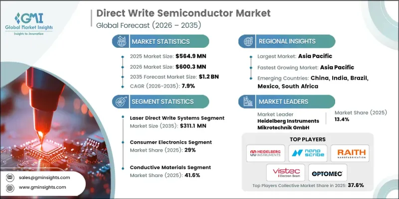
The Global Direct Write Semiconductor Market was valued at USD 564.9 million in 2025 and is estimated to grow at a CAGR of 7.9% to reach USD 1.2 billion by 2035.
Growth in the direct write semiconductor industry is largely driven by the increasing requirement for faster, highly accurate, and cost-efficient semiconductor manufacturing technologies. Direct write techniques are gaining momentum as manufacturers seek alternatives that improve design flexibility while reducing production complexity. Maskless lithography and advanced patterning solutions are playing a central role in this transformation by enabling faster device development cycles and improving manufacturing precision. These technologies help semiconductor developers accelerate prototyping processes, minimize material losses, and enhance the efficiency of fabrication workflows. In addition, the increasing shift toward next-generation electronic devices is creating a strong demand for manufacturing solutions capable of supporting compact and multifunctional component designs. Direct writing technology allows manufacturers to deposit conductive and semiconductive materials with high accuracy, enabling the development of complex circuits with superior resolution. This capability also allows researchers and manufacturers to explore new device architectures and innovative design possibilities. The direct write semiconductor market is also benefiting from the rising adoption of hybrid fabrication approaches that combine direct writing processes with traditional semiconductor production methods. Such approaches enable manufacturers to create highly customized and multi-layer electronic components with improved functionality. Furthermore, the increasing focus on on-demand manufacturing and limited-volume production is supporting the adoption of direct write technologies in research environments and specialized electronics development.
| Market Scope | |
|---|---|
| Start Year | 2025 |
| Forecast Year | 2026-2035 |
| Start Value | $564.9 Million |
| Forecast Value | $1.2 Billion |
| CAGR | 7.9% |
The laser direct write systems segment is projected to reach USD 311.1 million by 2035. Laser-based direct writing systems are gaining considerable attention due to their ability to deliver exceptional accuracy, high processing speed, and versatile patterning capabilities. These systems allow manufacturers to create intricate circuit structures at microscales without relying on conventional mask-based fabrication techniques. The ability to generate complex patterns directly on substrates significantly improves production flexibility and shortens development timelines. Laser-enabled direct writing solutions are particularly valuable in advanced electronics manufacturing because they support rapid prototyping and enable frequent design modifications during development stages.
The conductive materials segment accounted for 41.6% share in 2025, reflecting its significant importance within the overall industry ecosystem. Conductive materials play a vital role in the formation of high-precision circuits and interconnect structures that are essential for modern electronic components. Their strong electrical performance, adaptability across different substrate materials, and compatibility with direct writing processes make them a preferred choice for manufacturers working on advanced microelectronic applications. The increasing focus on high-performance electronic systems is further strengthening demand for conductive materials capable of supporting stable and reliable electrical pathways. In addition, the ability of these materials to support efficient current transmission and reduce electrical resistance makes them highly suitable for scaling direct write fabrication processes.
Europe Direct Write Semiconductor Market generated USD 96.4 million in 2025. The Europe direct write semiconductor industry is progressing as regional authorities place increasing emphasis on strengthening domestic semiconductor manufacturing capabilities. Policy-driven initiatives are encouraging technological innovation and supporting the expansion of advanced semiconductor production infrastructure across the region. Strategic collaboration among industry participants, research organizations, and government institutions is also contributing to the development of next-generation semiconductor fabrication technologies. These efforts are focused on improving supply chain resilience, enhancing technological competitiveness, and supporting long-term growth within the semiconductor ecosystem. As a result, the adoption of advanced patterning and additive manufacturing technologies is gradually expanding, reinforcing the region's role in the evolving direct write semiconductor market.
Key companies operating in the Global Direct Write Semiconductor Market include Raith GmbH, Vistec Electron Beam GmbH, Heidelberg Instruments Mikrotechnik GmbH, JEOL Ltd., Elionix Inc., SUSS MicroTec SE, Nanoscribe GmbH & Co. KG, Eulitha AG, Crestec Corporation, KLOE SAS, Holmarc Opto-Mechatronics Ltd., and HTL Co. Japan Ltd., Microlight3D SAS, NanoSystem Solutions, Inc., SVG Optronics Co., Ltd, and Optomec Inc. Companies active in the Global Direct Write Semiconductor Market are adopting several strategic initiatives to strengthen their competitive position and expand their technological capabilities. Many firms are increasing investment in research and development to enhance the precision, speed, and efficiency of direct writing technologies. Product innovation is another key strategy, with companies focusing on the development of advanced systems capable of supporting high-resolution semiconductor fabrication and complex circuit patterning. Strategic partnerships with research institutions and semiconductor manufacturers are also becoming more common as companies aim to accelerate technology development and expand commercial applications. Additionally, market participants are emphasizing the integration of advanced materials and software-driven design tools to improve system performance.
Table of Contents
Chapter 1 Methodology and Scope
- 1.1 Market scope and definition
- 1.2 Research design
- 1.2.1 Research approach
- 1.2.2 Data collection methods
- 1.3 Data mining sources
- 1.3.1 Global
- 1.3.2 Regional/Country
- 1.4 Base estimates and calculations
- 1.4.1 Base year calculation
- 1.4.2 Key trends for market estimation
- 1.5 Primary research and validation
- 1.5.1 Primary sources
- 1.6 Forecast model
- 1.7 Research assumptions and limitations
Chapter 2 Executive Summary
- 2.1 Industry 360° synopsis, 2021 - 2034
- 2.2 Key market trends
- 2.2.1 Technology/equipment type trends
- 2.2.2 Material type trends
- 2.2.3 Substrate trends
- 2.2.4 Application trends
- 2.2.5 End-user industry trends
- 2.2.6 Regional trends
- 2.3 TAM analysis, 2025-2034
- 2.4 CXO perspectives: Strategic imperatives
- 2.4.1 Executive decision points
- 2.4.2 Critical success factors
- 2.5 Future outlook and strategic recommendations
Chapter 3 Industry Insights
- 3.1 Industry ecosystem analysis
- 3.1.1 Supplier landscape
- 3.1.2 Profit margin analysis
- 3.1.3 Cost structure
- 3.1.4 Value addition at each stage
- 3.1.5 Factor affecting the value chain
- 3.1.6 Disruptions
- 3.2 Industry impact forces
- 3.2.1 Growth drivers
- 3.2.1.1 Increasing demand for advanced and custom semiconductor solutions
- 3.2.1.2 Expansion of flexible, wearable, and printed electronics applications
- 3.2.1.3 Rapid prototyping and reduced time-to-market requirements
- 3.2.1.4 Integration with additive manufacturing and advanced materials
- 3.2.1.5 Advancement in maskless lithography technologies for semiconductor packaging
- 3.2.2 Industry pitfalls and challenges
- 3.2.2.1 High initial capital expenditure and equipment costs
- 3.2.2.2 Limited standardization of direct writing processes
- 3.2.3 Market opportunities
- 3.2.3.1 Adoption in heterogeneous integration and system-in-package (SIP)
- 3.2.3.2 AI-enabled process optimization and automation
- 3.2.1 Growth drivers
- 3.3 Regulatory landscape
- 3.3.1 North America
- 3.3.2 Europe
- 3.3.3 Asia Pacific
- 3.3.4 Latin America
- 3.3.5 Middle East & Africa
- 3.4 Porter's analysis
- 3.5 PESTEL analysis
- 3.6 Technology and innovation landscape
- 3.6.1 Current technological trends
- 3.6.2 Emerging technologies
- 3.7 Emerging business models
- 3.8 Compliance requirements
- 3.9 Patent and IP analysis
- 3.10 Geopolitical and trade dynamics
Chapter 4 Competitive Landscape, 2024
- 4.1 Introduction
- 4.2 Company market share analysis
- 4.2.1 By region
- 4.2.1.1 North America
- 4.2.1.2 Europe
- 4.2.1.3 Asia Pacific
- 4.2.1.4 Latin America
- 4.2.1.5 Middle East & Africa
- 4.2.1 By region
- 4.3 Competitive benchmarking of key players
- 4.3.1 Financial performance comparison
- 4.3.1.1 Revenue
- 4.3.1.2 Profit margin
- 4.3.1.3 R&D
- 4.3.2 Product portfolio comparison
- 4.3.2.1 Product range breadth
- 4.3.2.2 Technology
- 4.3.2.3 Innovation
- 4.3.3 Geographic presence comparison
- 4.3.3.1 Global footprint analysis
- 4.3.3.2 Service network coverage
- 4.3.3.3 Market penetration by region
- 4.3.4 Competitive positioning matrix
- 4.3.4.1 Leaders
- 4.3.4.2 Challengers
- 4.3.4.3 Followers
- 4.3.4.4 Niche players
- 4.3.5 Strategic outlook matrix
- 4.3.1 Financial performance comparison
- 4.4 Key developments, 2021-2024
- 4.4.1 Mergers and acquisitions
- 4.4.2 Partnerships and collaborations
- 4.4.3 Technological advancements
- 4.4.4 Expansion and investment strategies
- 4.4.5 Digital transformation initiatives
- 4.5 Emerging/ startup competitors landscape
Chapter 5 Market Estimates and Forecast, By Technology / Equipment Type, 2022 - 2035 ($ Mn)
- 5.1 Key trends
- 5.2 Material deposition systems
- 5.2.1 Low-viscosity inkjet systems
- 5.2.2 Medium-viscosity aerosol jet systems
- 5.2.3 High-viscosity micro-dispensing systems
- 5.3 Laser direct write systems
- 5.3.1 Spatial light modulator (SLM/DMD-Based)
- 5.3.2 Direct laser scanning systems
- 5.3.3 Two-photon polymerization systems
- 5.4 Electron beam direct write systems
- 5.5 Thermal scanning probe lithography systems
Chapter 6 Market Estimates and Forecast, By Material Type, 2022 - 2035 ($ Mn)
- 6.1 Key trends
- 6.2 Conductive materials
- 6.3 Semiconductor materials
- 6.4 Dielectric & insulating materials
- 6.5 Functional composite materials
Chapter 7 Market Estimates and Forecast, By Substrate, 2022 - 2035 ($ Mn)
- 7.1 Key trends
- 7.2 Flexible substrates
- 7.3 Rigid substrates
- 7.4 Conformal/3D substrates
Chapter 8 Market Estimates and Forecast, By Application, 2022 - 2035 ($ Mn)
- 8.1 Key trends
- 8.2 Advanced packaging & interconnects
- 8.3 Flexible & printed electronics
- 8.4 Mems & sensors
- 8.5 Antennas & RF components
- 8.6 Biomedical & healthcare devices
- 8.7 Others
Chapter 9 Market Estimates and Forecast, By End-User Industry, 2022 - 2035 ($ Mn)
- 9.1 Key trends
- 9.2 Aerospace & defense
- 9.3 Automotive
- 9.4 Consumer electronics
- 9.5 Healthcare & medical devices
- 9.6 Telecommunications & 5G
- 9.7 Others
Chapter 10 Market Estimates and Forecast, By Region, 2022 - 2035 ($ Mn)
- 10.1 Key trends
- 10.2 North America
- 10.2.1 U.S.
- 10.2.2 Canada
- 10.3 Europe
- 10.3.1 Germany
- 10.3.2 UK
- 10.3.3 France
- 10.3.4 Spain
- 10.3.5 Italy
- 10.3.6 Netherlands
- 10.4 Asia Pacific
- 10.4.1 China
- 10.4.2 India
- 10.4.3 Japan
- 10.4.4 Australia
- 10.4.5 South Korea
- 10.5 Latin America
- 10.5.1 Brazil
- 10.5.2 Mexico
- 10.5.3 Argentina
- 10.6 Middle East and Africa
- 10.6.1 South Africa
- 10.6.2 Saudi Arabia
- 10.6.3 UAE
Chapter 11 Company Profiles
- 11.1 Global Key Players
- 11.1.1 Raith GmbH
- 11.1.2 Heidelberg Instruments Mikrotechnik GmbH
- 11.1.3 JEOL Ltd.
- 11.1.4 Optomec Inc.
- 11.2 Regional Key Players
- 11.2.1 North America
- 11.2.1.1 NanoSystem Solutions, Inc.
- 11.2.1.2 SVG Optronics Co., Ltd
- 11.2.1.3 Nanoscribe GmbH & Co. KG
- 11.2.2 Europe
- 11.2.2.1 Vistec Electron Beam GmbH
- 11.2.2.2 SUSS MicroTec SE
- 11.2.2.3 Eulitha AG
- 11.2.3 APAC
- 11.2.3.1 Elionix Inc.
- 11.2.3.2 Crestec Corporation
- 11.2.3.3 HTL Co. Japan Ltd.
- 11.2.1 North America
- 11.3 Niche Players / Disruptors
- 11.3.1 KLOE SAS
- 11.3.2 Holmarc Opto-Mechatronics Ltd.
- 11.3.3 Microlight3D SAS

