
PUBLISHER: Global Market Insights Inc. | PRODUCT CODE: 2019126

PUBLISHER: Global Market Insights Inc. | PRODUCT CODE: 2019126
Semiconductor Metrology and Inspection Market Opportunity, Growth Drivers, Industry Trend Analysis, and Forecast 2026 - 2035
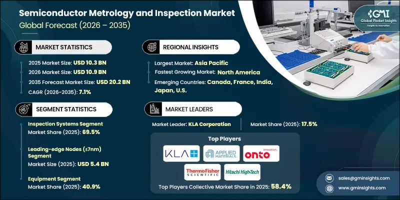
The Global Semiconductor Metrology and Inspection Market was valued at USD 10.3 billion in 2025 and is estimated to grow at a CAGR of 7.1% to reach USD 20.2 billion by 2035.
Market expansion is fueled by the increasing complexity of advanced semiconductor nodes, the adoption of EUV and High-NA lithography, and the rising demand for AI and machine learning chips. The shift toward 3D NAND and GAA architectures is also driving the need for precise metrology and inspection solutions. Advanced packaging and multi-layer semiconductor structures require high-resolution, reliable inspection systems to manage stochastic defects and maintain yield. Growth is further supported by increasing foundry capacities in APAC and the widespread adoption of hybrid metrology solutions in high-volume manufacturing facilities. Technological advancements are enabling more accurate nanoscale measurements, improving process control, and minimizing defect-related losses, which is critical for high-performance computing and next-generation semiconductor production.
| Market Scope | |
|---|---|
| Start Year | 2025 |
| Forecast Year | 2026-2035 |
| Start Value | $10.3 Billion |
| Forecast Value | $20.2 Billion |
| CAGR | 7.1% |
The increasing adoption of EUV lithography is a major driver of the semiconductor metrology and inspection market, particularly for sub-7nm nodes where stochastic defects and pattern variability demand ultra-high-resolution inspection systems. The growing requirement for AI/ML chips necessitates tighter process control, as even minor nanoscale variations can disrupt device efficiency and output. Rising production of advanced packaging solutions, scaling to sub-5nm nodes, and multi-layer inspection needs are key factors supporting market growth. The integration of hybrid metrology in high-volume fabs allows for faster, more accurate measurements, ensuring yield optimization and process consistency across complex manufacturing environments.
The inspection systems segment held a 69.5% share in 2025. These systems are crucial for detecting defects across wafers, masks, and packaging layers with high precision. Inspection platforms play a vital role in yield enhancement, process monitoring, and compliance with stringent advanced-node manufacturing standards. They allow semiconductor manufacturers to identify, analyze, and mitigate defects efficiently across high-volume production lines, making them an essential investment for fabs aiming to maintain competitiveness in high-performance and AI chip production.
The leading-edge nodes segment (<=7nm) held a market value of USD 5.4 billion in 2025, reflecting high demand for advanced metrology and inspection solutions. These cutting-edge nodes require extremely precise measurements to support EUV lithography, multi-patterning techniques, and GAA or FinFET architectures. Tight defect tolerances and complex production processes make advanced inspection and metrology systems indispensable for ensuring yield, device performance, and competitiveness in high-end computing applications.
North America Semiconductor Metrology and Inspection Market accounted for 31.6% share in 2025. Growth in this region is driven by a strong focus on domestic semiconductor manufacturing and process precision. The adoption of AI-driven inspection systems, hybrid metrology solutions, and in-line process monitoring supports advanced nodes and high-volume production facilities. Government initiatives, collaborative research, and industry partnerships are accelerating innovation in critical dimension measurement, defect detection, and multi-layer analysis. North American fabs emphasize precision, throughput optimization, and yield improvement, positioning the region as a leader in next-generation metrology and inspection technologies.
Key players operating in the Global Semiconductor Metrology and Inspection Market include Advantest Corporation, Applied Materials, Inc., ASML Holding N.V, Bruker Corporation, Camtek Ltd., Hitachi Ltd., JEOL Ltd., KLA Corporation, Lasertec Corporation, Nikon Corporation, Nova Measuring Instruments Ltd., Olympus (EVIDENT), Onto Innovation, Inc., Park Systems Corp., Thermo Fisher Scientific Inc., Toray Engineering Co., Ltd., and Zygo Corporation. Companies in the Semiconductor Metrology and Inspection Market are implementing strategies to strengthen market presence and expand global reach. They are investing in research and development to improve inspection resolution, metrology accuracy, and process integration for advanced nodes. Partnerships with semiconductor foundries, fabless companies, and equipment manufacturers enhance collaborative innovation and adoption of hybrid solutions. Firms are also focusing on expanding service portfolios, including in-line process control, predictive maintenance, and data analytics, to increase value for high-volume fabs. Geographic expansion, particularly in APAC and North America, ensures access to growing production facilities.
Table of Contents
Chapter 1 Methodology and Scope
- 1.1 Market scope and definition
- 1.2 Research design
- 1.2.1 Research approach
- 1.2.2 Data collection methods
- 1.3 Data mining sources
- 1.3.1 Global
- 1.3.2 Regional/Country
- 1.4 Base estimates and calculations
- 1.4.1 Base year calculation
- 1.4.2 Key trends for market estimation
- 1.5 Primary research and validation
- 1.5.1 Primary sources
- 1.6 Forecast model
- 1.7 Research assumptions and limitations
Chapter 2 Executive Summary
- 2.1 Industry 360° synopsis, 2022 - 2035
- 2.2 Key market trends
- 2.2.1 Equipment type trends
- 2.2.2 Measurement parameter trends
- 2.2.3 Node technology trends
- 2.2.4 Offering type trends
- 2.2.5 Application trends
- 2.2.6 End-user type trends
- 2.2.7 Regional trends
- 2.3 TAM Analysis, 2026-2035
- 2.4 CXO perspectives: Strategic imperatives
Chapter 3 Industry Insights
- 3.1 Industry ecosystem analysis
- 3.1.1 Supplier Landscape
- 3.1.2 Profit Margin
- 3.1.3 Cost structure
- 3.1.4 Value addition at each stage
- 3.1.5 Factor affecting the value chain
- 3.1.6 Disruptions
- 3.2 Industry impact forces
- 3.2.1 Growth drivers
- 3.2.1.1 EUV lithography complexity requires advanced inspection precision
- 3.2.1.2 Sub-5nm nodes increase defect density sensitivity
- 3.2.1.3 3D NAND and GAA architectures need multi-layer metrology
- 3.2.1.4 Automotive chips demand zero-defect manufacturing standards
- 3.2.1.5 AI/ML chips require tighter process control tolerances
- 3.2.2 Industry pitfalls and challenges
- 3.2.2.1 High capital cost limits SME adoption
- 3.2.2.2 Tool throughput constraints in high-volume fabs
- 3.2.3 Market opportunities
- 3.2.3.1 Growth in heterogeneous and chiplet packaging inspection
- 3.2.3.2 Emerging fabs in India and Southeast Asia demand tools
- 3.2.1 Growth drivers
- 3.3 Growth potential analysis
- 3.4 Regulatory landscape
- 3.4.1 North America
- 3.4.2 Europe
- 3.4.3 Asia Pacific
- 3.4.4 Latin America
- 3.4.5 Middle East & Africa
- 3.5 Porter's analysis
- 3.6 PESTEL analysis
- 3.7 Technology and Innovation landscape
- 3.7.1 Current technological trends
- 3.7.2 Emerging technologies
- 3.8 Price trends
- 3.8.1 By region
- 3.8.2 By product
- 3.9 Pricing Strategies
- 3.10 Emerging Business Models
- 3.11 Compliance Requirements
- 3.12 Patent and IP analysis
Chapter 4 Competitive Landscape, 2025
- 4.1 Introduction
- 4.2 Company market share analysis
- 4.2.1 By region
- 4.2.1.1 North America
- 4.2.1.2 Europe
- 4.2.1.3 Asia Pacific
- 4.2.1.4 Latin America
- 4.2.1.5 Middle East & Africa
- 4.2.2 Market concentration analysis
- 4.2.1 By region
- 4.3 Competitive benchmarking of key players
- 4.3.1 Financial performance comparison
- 4.3.1.1 Revenue
- 4.3.1.2 Profit margin
- 4.3.1.3 R&D
- 4.3.2 Product portfolio comparison
- 4.3.2.1 Product range breadth
- 4.3.2.2 Technology
- 4.3.2.3 Innovation
- 4.3.3 Geographic presence comparison
- 4.3.3.1 Global footprint analysis
- 4.3.3.2 Service network coverage
- 4.3.3.3 Market penetration by region
- 4.3.4 Competitive positioning matrix
- 4.3.4.1 Leaders
- 4.3.4.2 Challengers
- 4.3.4.3 Followers
- 4.3.4.4 Niche players
- 4.3.5 Strategic outlook matrix
- 4.3.1 Financial performance comparison
- 4.4 Key developments
- 4.4.1 Mergers and acquisitions
- 4.4.2 Partnerships and collaborations
- 4.4.3 Technological advancements
- 4.4.4 Expansion and investment strategies
- 4.4.5 Digital transformation initiatives
- 4.5 Emerging/ startup competitors landscape
Chapter 5 Market Estimates and Forecast, By Equipment Type, 2022 - 2035 (USD Million)
- 5.1 Key trends
- 5.2 Metrology systems
- 5.2.1 Optical metrology
- 5.2.2 E-beam metrology
- 5.2.3 X-ray metrology
- 5.2.4 AFM & others
- 5.3 Inspection systems
- 5.3.1 Wafer inspection
- 5.3.2 Mask/reticle inspection
Chapter 6 Market Estimates and Forecast, By Measurement Parameter, 2022 - 2035 (USD Million)
- 6.1 Key trends
- 6.2 Critical dimension (CD) metrology
- 6.3 Overlay metrology
- 6.4 Film thickness & material metrology
- 6.5 Others
Chapter 7 Market Estimates and Forecast, By Node Technology, 2022 - 2035 (USD Million)
- 7.1 Key trends
- 7.2 Leading-edge nodes (<=7nm)
- 7.3 Advanced nodes (8-28nm)
- 7.4 Mature nodes (>28nm)
Chapter 8 Market Estimates and Forecast, By Offering Type, 2022 - 2035 (USD Million)
- 8.1 Key trends
- 8.2 Equipment
- 8.3 Software
- 8.4 Services
Chapter 9 Market Estimates and Forecast, By Application, 2022 - 2035 (USD Million)
- 9.1 Key trends
- 9.2 Wafer fabrication
- 9.2.1 Inline control
- 9.2.2 Offline control
- 9.3 Mask/reticle fabrication
- 9.3.1 Inline control
- 9.3.2 Offline control
- 9.4 Advanced Packaging
- 9.4.1 Wafer-level packaging (WLP)
- 9.4.2 3D IC
- 9.4.3 Panel-level packaging
Chapter 10 Market Estimates and Forecast, By End-User Type, 2022 - 2035 (USD Million)
- 10.1 Key trends
- 10.2 IDMs
- 10.3 Pure-play foundries
- 10.4 OSATs
Chapter 11 Market Estimates and Forecast, By Region, 2022 - 2035 (USD Million)
- 11.1 Key trends
- 11.2 North America
- 11.2.1 U.S.
- 11.2.2 Canada
- 11.3 Europe
- 11.3.1 Germany
- 11.3.2 UK
- 11.3.3 France
- 11.3.4 Spain
- 11.3.5 Italy
- 11.4 Asia Pacific
- 11.4.1 China
- 11.4.2 India
- 11.4.3 Japan
- 11.4.4 Australia
- 11.4.5 South Korea
- 11.5 Latin America
- 11.5.1 Brazil
- 11.5.2 Mexico
- 11.5.3 Argentina
- 11.6 Middle East and Africa
- 11.6.1 South Africa
- 11.6.2 Saudi Arabia
- 11.6.3 UAE
Chapter 12 Company Profiles
- 12.1 Global Key Players
- 12.1.1 Applied Materials, Inc.
- 12.1.2 ASML Holding N.V
- 12.1.3 KLA Corporation
- 12.1.4 Hitachi Ltd.
- 12.1.5 Thermo Fisher Scientific Inc.
- 12.2 Regional key players
- 12.2.1 North America
- 12.2.1.1 Advantest Corporation
- 12.2.1.2 Bruker Corporation
- 12.2.1.3 Onto Innovation, Inc
- 12.2.1.4 Nova Measuring Instruments Ltd.
- 12.2.2 Asia Pacific
- 12.2.2.1 JEOL Ltd.
- 12.2.2.2 Nikon Corporation
- 12.2.2.3 Lasertec Corporation
- 12.2.2.4 Toray Engineering Co., Ltd.
- 12.2.2.5 Park Systems Corp.
- 12.2.3 Europe
- 12.2.3.1 Camtek Ltd.
- 12.2.3.2 Olympus (EVIDENT)
- 12.2.3.3 Zygo Corporation
- 12.2.1 North America

