
PUBLISHER: Global Market Insights Inc. | PRODUCT CODE: 2019172

PUBLISHER: Global Market Insights Inc. | PRODUCT CODE: 2019172
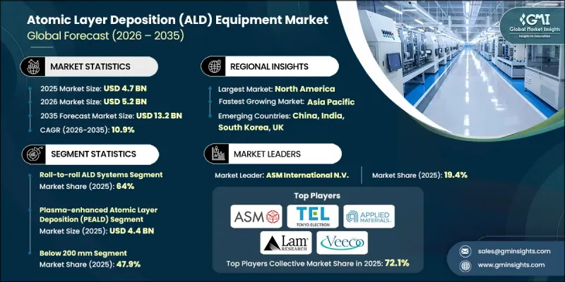
Atomic Layer Deposition (ALD) Equipment Market Opportunity, Growth Drivers, Industry Trend Analysis, and Forecast 2026 - 2035
The Global Atomic Layer Deposition Equipment Market was valued at USD 4.7 billion in 2025 and is estimated to grow at a CAGR of 10.9% to reach USD 13.2 billion by 2035.
Growth across the atomic layer deposition equipment market is being driven by the accelerating shift toward advanced semiconductor manufacturing nodes, where precision at the atomic level is essential for device performance and reliability. The expansion of next-generation memory architectures and the growing demand for high-efficiency power electronics are significantly contributing to market demand. In addition, increasing integration of ALD technologies in nanoscale device fabrication and advanced packaging solutions is strengthening industry growth. Rising investments in semiconductor fabrication facilities, coupled with the need for high-performance materials, are reinforcing the importance of ALD systems. The market is also benefiting from the adoption of innovative manufacturing techniques that require consistent thin-film deposition across complex structures, supporting the evolution of modern electronics and ensuring long-term industry expansion.
| Market Scope | |
|---|---|
| Start Year | 2025 |
| Forecast Year | 2026-2035 |
| Start Value | $4.7 Billion |
| Forecast Value | $13.2 Billion |
| CAGR | 10.9% |
The atomic layer deposition equipment market continues to gain traction from the rising demand for advanced semiconductor fabrication processes. As manufacturers move toward smaller and more complex nodes, precise control over material deposition becomes increasingly critical. The growing adoption of wide-bandgap semiconductor materials is further accelerating demand for high-quality deposition systems. These materials require reliable thin-film coatings to ensure optimal performance in high-power and high-frequency applications. Additionally, the increasing role of ALD technology in advanced packaging and micro-scale device production is enhancing its adoption across multiple end-use industries. Continuous innovation in fabrication technologies and increased capital spending on semiconductor manufacturing infrastructure are further strengthening the market outlook.
The single-wafer ALD systems segment is expected to grow at a CAGR of 10.2% through 2035, supported by rising demand for highly controlled and flexible deposition processes. These systems offer precise film thickness control and adaptability for complex device architectures, making them highly suitable for next-generation semiconductor manufacturing. Their ability to support multiple material layers and advanced chip designs continues to drive adoption across high-performance computing and memory applications. The segment benefits from increasing requirements for customization and precision in fabrication processes, reinforcing its role in the evolving semiconductor landscape.
The plasma-enhanced atomic layer deposition segment reached USD 4.4 billion in 2025. Its strong market presence is attributed to its capability to deposit high-quality thin films at comparatively lower temperatures, making it suitable for sensitive substrates and advanced device structures. The technology supports improved film properties, enhanced uniformity, and better integration with complex semiconductor architectures. Its compatibility with advanced manufacturing requirements continues to sustain demand across high-end fabrication environments, positioning it as a critical component within the broader atomic layer deposition equipment market.
North America Atomic Layer Deposition Equipment Market accounted for 36.5% share in 2025, driven by increasing investments in semiconductor manufacturing and advanced materials research. The region is witnessing growing demand for high-performance computing technologies, which is accelerating the adoption of precision deposition equipment. Expanding manufacturing capabilities and continuous technological advancements are supporting regional growth. In addition, a strong focus on innovation and development of next-generation semiconductor solutions is further contributing to the expansion of the market. Ongoing investments in fabrication facilities and materials engineering are expected to maintain the region's competitive position over the forecast period.
Key players in the Global Atomic Layer Deposition Equipment Market Aixtron SE, ANRIC Technologies, Applied Materials Inc., Arradiance LLC, ASM International NV, Beneq Oy, Cambridge NanoTech, CVD Equipment Corporation, Entegris Inc., Forge Nano Inc., Hitachi High-Technologies Corporation, Kurt J. Lesker Company, Lam Research Corporation, Meyer Burger, MSE Supplies LLC, Nano-Master Inc., Oxford Instruments plc, Picosun Oy, Radiation Monitoring Devices Inc., SENTECH Instruments GmbH, SHOWA SHINKU CO. LTD., SVT Associates, Tokyo Electron Limited, Veeco Instruments Inc., Watty Corporation. Companies operating in the atomic layer deposition equipment market are focusing on strengthening their market position through continuous technological innovation, strategic collaborations, and expansion of production capabilities. They are investing heavily in research and development to enhance deposition precision, improve throughput, and develop advanced materials compatible with next-generation semiconductor nodes. Partnerships with semiconductor manufacturers and research institutions are enabling companies to co-develop tailored solutions that meet evolving industry requirements. Firms are also expanding their global footprint by establishing new manufacturing facilities and strengthening supply chain networks to ensure consistent product availability. Additionally, companies are prioritizing product differentiation through improved efficiency, reduced operational costs, and enhanced system integration capabilities.
Table of Contents
Chapter 1 Methodology and Scope
- 1.1 Market scope and definition
- 1.2 Research design
- 1.2.1 Research approach
- 1.2.2 Data collection methods
- 1.3 Data mining sources
- 1.3.1 Global
- 1.3.2 Regional/Country
- 1.4 Base estimates and calculations
- 1.4.1 Base year calculation
- 1.4.2 Key trends for market estimation
- 1.5 Primary research and validation
- 1.5.1 Primary sources
- 1.6 Forecast model
- 1.7 Research assumptions and limitations
Chapter 2 Executive Summary
- 2.1 Industry 360° synopsis, 2022 - 2035
- 2.2 Key market trends
- 2.2.1 Equipment type trends
- 2.2.2 Technology type trends
- 2.2.3 Wafer size trends
- 2.2.4 Application trends
- 2.2.5 End-user industry trends
- 2.2.6 Regional trends
- 2.3 TAM Analysis, 2026-2035
- 2.4 CXO perspectives: Strategic imperatives
Chapter 3 Industry Insights
- 3.1 Industry ecosystem analysis
- 3.1.1 Supplier Landscape
- 3.1.2 Profit Margin
- 3.1.3 Cost structure
- 3.1.4 Value addition at each stage
- 3.1.5 Factor affecting the value chain
- 3.1.6 Disruptions
- 3.2 Industry impact forces
- 3.2.1 Growth drivers
- 3.2.1.1 Rising demand for advanced semiconductor node fabrication
- 3.2.1.2 Growth in power electronics and wide-bandgap semiconductors
- 3.2.1.3 Growing adoption of high-k dielectric materials in chips
- 3.2.1.4 Expansion of 3D NAND and DRAM memory production
- 3.2.1.5 Demand for conformal coatings in complex semiconductor structures
- 3.2.2 Industry pitfalls and challenges
- 3.2.2.1 High capital cost of ALD equipment systems
- 3.2.2.2 Slow deposition rates compared to alternative techniques
- 3.2.3 Market opportunities
- 3.2.3.1 Increasing ALD adoption in advanced packaging technologies
- 3.2.3.2 Growing applications in MEMS and nanoscale devices
- 3.2.1 Growth drivers
- 3.3 Growth potential analysis
- 3.4 Regulatory landscape
- 3.4.1 North America
- 3.4.2 Europe
- 3.4.3 Asia Pacific
- 3.4.4 Latin America
- 3.4.5 Middle East & Africa
- 3.5 Porter's analysis
- 3.6 PESTEL analysis
- 3.7 Technology and Innovation landscape
- 3.7.1 Current technological trends
- 3.7.2 Emerging technologies
- 3.8 Price trends
- 3.8.1 By region
- 3.8.2 By product
- 3.9 Pricing Strategies
- 3.10 Emerging Business Models
- 3.11 Compliance Requirements
- 3.12 Patent and IP analysis
Chapter 4 Competitive Landscape, 2025
- 4.1 Introduction
- 4.2 Company market share analysis
- 4.2.1 By region
- 4.2.1.1 North America
- 4.2.1.2 Europe
- 4.2.1.3 Asia Pacific
- 4.2.1.4 Latin America
- 4.2.1.5 Middle East & Africa
- 4.2.2 Market concentration analysis
- 4.2.1 By region
- 4.3 Competitive benchmarking of key players
- 4.3.1 Financial performance comparison
- 4.3.1.1 Revenue
- 4.3.1.2 Profit margin
- 4.3.1.3 R&D
- 4.3.2 Product portfolio comparison
- 4.3.2.1 Product range breadth
- 4.3.2.2 Technology
- 4.3.2.3 Innovation
- 4.3.3 Geographic presence comparison
- 4.3.3.1 Global footprint analysis
- 4.3.3.2 Service network coverage
- 4.3.3.3 Market penetration by region
- 4.3.4 Competitive positioning matrix
- 4.3.4.1 Leaders
- 4.3.4.2 Challengers
- 4.3.4.3 Followers
- 4.3.4.4 Niche players
- 4.3.5 Strategic outlook matrix
- 4.3.1 Financial performance comparison
- 4.4 Key developments
- 4.4.1 Mergers and acquisitions
- 4.4.2 Partnerships and collaborations
- 4.4.3 Technological advancements
- 4.4.4 Expansion and investment strategies
- 4.4.5 Digital transformation initiatives
- 4.5 Emerging/ startup competitors landscape
Chapter 5 Market Estimates and Forecast, By Equipment Type, 2022 - 2035 (USD Million)
- 5.1 Key trends
- 5.2 Single-wafer ALD systems
- 5.3 Batch ALD systems
- 5.4 Spatial ALD systems
- 5.5 Roll-to-roll ALD systems
Chapter 6 Market Estimates and Forecast, By Technology Type, 2022 - 2035 (USD Million)
- 6.1 Key trends
- 6.2 Thermal ALD
- 6.3 Plasma-enhanced ALD (PEALD)
Chapter 7 Market Estimates and Forecast, By Wafer Size, 2022 - 2035 (USD Million)
- 7.1 Key trends
- 7.2 300 mm
- 7.3 200 mm
- 7.4 Below 200 mm
Chapter 8 Market Estimates and Forecast, By Application, 2022 - 2035 (USD Million)
- 8.1 Key trends
- 8.2 Logic & memory devices
- 8.3 MEMS & sensors
- 8.4 Power electronics
- 8.5 Optoelectronics
- 8.6 Energy storage
Chapter 9 Market Estimates and Forecast, By End-User Industry, 2022 - 2035 (USD Million)
- 9.1 Key trends
- 9.2 Semiconductor manufacturers
- 9.3 Electronics & optoelectronics manufacturers
- 9.4 Energy & battery manufacturers
- 9.5 Research institutions
- 9.6 Others
Chapter 10 Market Estimates and Forecast, By Region, 2022 - 2035 (USD Million)
- 10.1 Key trends
- 10.2 North America
- 10.2.1 U.S.
- 10.2.2 Canada
- 10.3 Europe
- 10.3.1 Germany
- 10.3.2 UK
- 10.3.3 France
- 10.3.4 Spain
- 10.3.5 Italy
- 10.3.6 Netherlands
- 10.4 Asia Pacific
- 10.4.1 China
- 10.4.2 India
- 10.4.3 Japan
- 10.4.4 Australia
- 10.4.5 South Korea
- 10.5 Latin America
- 10.5.1 Brazil
- 10.5.2 Mexico
- 10.5.3 Argentina
- 10.6 Middle East and Africa
- 10.6.1 South Africa
- 10.6.2 Saudi Arabia
- 10.6.3 UAE
Chapter 11 Company Profiles
- 11.1 Global Key Players
- 11.1.1 Applied Materials, Inc.
- 11.1.2 ASM International NV
- 11.1.3 Lam Research Corporation
- 11.1.4 Tokyo Electron Limited
- 11.1.5 Veeco Instruments Inc.
- 11.2 Regional key players
- 11.2.1 North America
- 11.2.1.1 Arradiance, LLC
- 11.2.1.2 CVD Equipment Corporation
- 11.2.1.3 Kurt J. Lesker Company
- 11.2.1.4 Nano-Master, Inc.
- 11.2.1.5 SVT Associates
- 11.2.2 Asia Pacific
- 11.2.2.1 Hitachi High-Technologies Corporation
- 11.2.2.2 SHOWA SHINKU CO., LTD.
- 11.2.2.3 Watty Corporation
- 11.2.3 Europe
- 11.2.3.1 Aixtron SE
- 11.2.3.2 Beneq Oy
- 11.2.3.3 Oxford Instruments plc
- 11.2.3.4 SENTECH Instruments GmbH
- 11.2.3.5 Meyer Burger
- 11.2.1 North America
- 11.3 Niche Players/Disruptors
- 11.3.1 ANRIC Technologies
- 11.3.2 Cambridge NanoTech
- 11.3.3 Entegris Inc.
- 11.3.4 Forge Nano Inc.
- 11.3.5 MSE Supplies LLC
- 11.3.6 Picosun Oy
- 11.3.7 Radiation Monitoring Devices, Inc.

