
PUBLISHER: Global Market Insights Inc. | PRODUCT CODE: 2038320

PUBLISHER: Global Market Insights Inc. | PRODUCT CODE: 2038320
Semiconductor Process Control Equipment Market Opportunity, Growth Drivers, Industry Trend Analysis, and Forecast 2026 - 2035
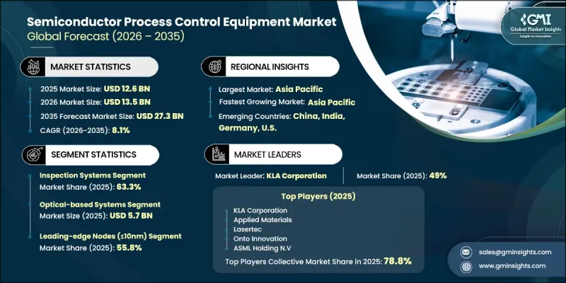
The Global Semiconductor Process Control Equipment Market was valued at USD 12.6 billion in 2025 and is estimated to grow at a CAGR of 8.1% to reach USD 27.3 billion by 2035.
Growth is supported by the increasing scale of semiconductor production and the growing need to maintain strict quality standards throughout fabrication. Manufacturers are prioritizing advanced process control solutions to reduce defects, maintain tighter tolerances, and enable continuous monitoring across production stages. The rising complexity of chip designs and manufacturing techniques is further accelerating demand for highly accurate inspection and metrology systems. In addition, the industry is benefiting from ongoing investments in fabrication capacity and technological upgrades. As semiconductor devices become more intricate, companies are placing greater emphasis on improving yield, enhancing process stability, and optimizing operational performance through data-driven manufacturing approaches and advanced equipment integration.
| Market Scope | |
|---|---|
| Start Year | 2025 |
| Forecast Year | 2026-2035 |
| Start Value | $12.6 Billion |
| Forecast Value | $27.3 Billion |
| CAGR | 8.1% |
The semiconductor process control equipment market is further strengthened by significant investments in fabrication infrastructure and expansion initiatives across the global semiconductor value chain. Increasing complexity in logic and memory manufacturing processes is creating greater sensitivity to defects, making process control equipment essential for maintaining production efficiency. Semiconductor manufacturers are focusing on improving defect detection capabilities, ensuring process consistency, and enhancing productivity across both fabrication and packaging stages. The rapid adoption of advanced manufacturing technologies and integration techniques is also contributing to higher demand for inspection and control systems.
The inspection systems segment accounted for 63.3% share in 2025. Their widespread use across multiple stages of semiconductor manufacturing supports early defect detection and helps maintain production yields. These systems play a critical role in identifying irregularities and ensuring that manufacturing processes remain within acceptable parameters.
The e-beam-based systems segment is anticipated to grow at a CAGR of 9.9% during 2026-2035. This growth is attributed to the increasing requirement for high-resolution analysis and precise measurement capabilities in semiconductor production. As device structures become more compact and complex, these systems are increasingly utilized to detect extremely small defects and provide detailed analysis that supports process optimization and yield improvement.
North America Semiconductor Process Control Equipment Market captured 28.5% share in 2025. The region is witnessing continued growth due to advancements in semiconductor manufacturing technologies and increased investment in fabrication facilities. Ongoing development of advanced production capabilities is driving demand for process control equipment that ensures consistency, improves operational efficiency, and supports high-performance manufacturing requirements.
Key companies operating in the Global Semiconductor Process Control Equipment Market include ASML Holding N.V., Applied Materials Inc., KLA Corporation, Tokyo Electron Limited, Hitachi High-Tech Corporation, Onto Innovation Inc., SCREEN Holdings Co., Ltd, Nova Ltd, Camtek Ltd, Advantest Corporation, Lasertec Corporation, Rudolph Technologies, ZEISS Group, Muetec Co., Ltd, and Multi-21 Solutions Limited. Companies in the Semiconductor Process Control Equipment Market are adopting a range of strategic initiatives to strengthen their competitive position and expand market presence. They are investing heavily in research and development to introduce advanced inspection and metrology solutions that address evolving manufacturing challenges. Many players are focusing on integrating data analytics and automation into their equipment to improve accuracy and operational efficiency. Strategic collaborations and partnerships are being pursued to enhance technological capabilities and broaden product portfolios. Additionally, companies are expanding their global footprint by establishing new facilities and strengthening supply chains to support growing demand.
Table of Contents
Chapter 1 Methodology and Scope
- 1.1 Market scope and definition
- 1.2 Research design
- 1.2.1 Research approach
- 1.2.2 Data collection methods
- 1.3 Data mining sources
- 1.3.1 Global
- 1.3.2 Regional/Country
- 1.4 Base estimates and calculations
- 1.4.1 Base year calculation
- 1.4.2 Key trends for market estimation
- 1.5 Primary research and validation
- 1.5.1 Primary sources
- 1.6 Forecast model
- 1.7 Research assumptions and limitations
Chapter 2 Executive Summary
- 2.1 Industry 360° synopsis, 2022 - 2035
- 2.2 Key market trends
- 2.2.1 Equipment type trends
- 2.2.2 Technology type trends
- 2.2.3 Application trends
- 2.2.4 Process node trends
- 2.2.5 End-user trends
- 2.2.6 Regional trends
- 2.3 TAM Analysis, 2026-2035
- 2.4 CXO perspectives: Strategic imperatives
Chapter 3 Industry Insights
- 3.1 Industry ecosystem analysis
- 3.1.1 Supplier Landscape
- 3.1.2 Profit Margin
- 3.1.3 Cost structure
- 3.1.4 Value addition at each stage
- 3.1.5 Factor affecting the value chain
- 3.1.6 Disruptions
- 3.2 Industry impact forces
- 3.2.1 Growth drivers
- 3.2.1.1 Increasing complexity at advanced semiconductor technology nodes
- 3.2.1.2 Rising investment in new fabs and capacity expansion worldwide
- 3.2.1.3 Growing emphasis on yield improvement and manufacturing efficiency
- 3.2.1.4 Expansion of advanced packaging and heterogeneous integration
- 3.2.1.5 Adoption of data-driven and automated manufacturing environments
- 3.2.2 Industry pitfalls and challenges
- 3.2.2.1 High capital intensity and rising cost of advanced process control tools
- 3.2.2.2 Increasing complexity of tool integration and data overload in fabs
- 3.2.3 Market opportunities
- 3.2.3.1 Expansion of AI-driven and advanced analytics-enabled process control solutions
- 3.2.3.2 Rising deployment of process control tools in advanced packaging and back-end manufacturing
- 3.2.1 Growth drivers
- 3.3 Growth potential analysis
- 3.4 Regulatory landscape
- 3.4.1 North America
- 3.4.2 Europe
- 3.4.3 Asia Pacific
- 3.4.4 Latin America
- 3.4.5 Middle East & Africa
- 3.5 Porter's analysis
- 3.6 PESTEL analysis
- 3.7 Technology and Innovation landscape
- 3.7.1 Current technological trends
- 3.7.2 Emerging technologies
- 3.8 Price trends
- 3.8.1 By region
- 3.8.2 By product
- 3.9 Pricing Strategies
- 3.10 Emerging Business Models
- 3.11 Compliance Requirements
- 3.12 Patent and IP analysis
Chapter 4 Competitive Landscape, 2025
- 4.1 Introduction
- 4.2 Company market share analysis
- 4.2.1 By region
- 4.2.1.1 North America
- 4.2.1.2 Europe
- 4.2.1.3 Asia Pacific
- 4.2.1.4 Latin America
- 4.2.1.5 Middle East & Africa
- 4.2.2 Market concentration analysis
- 4.2.1 By region
- 4.3 Competitive benchmarking of key players
- 4.3.1 Financial performance comparison
- 4.3.1.1 Revenue
- 4.3.1.2 Profit margin
- 4.3.1.3 R&D
- 4.3.2 Product portfolio comparison
- 4.3.2.1 Product range breadth
- 4.3.2.2 Technology
- 4.3.2.3 Innovation
- 4.3.3 Geographic presence comparison
- 4.3.3.1 Global footprint analysis
- 4.3.3.2 Service network coverage
- 4.3.3.3 Market penetration by region
- 4.3.4 Competitive positioning matrix
- 4.3.4.1 Leaders
- 4.3.4.2 Challengers
- 4.3.4.3 Followers
- 4.3.4.4 Niche players
- 4.3.5 Strategic outlook matrix
- 4.3.1 Financial performance comparison
- 4.4 Key developments
- 4.4.1 Mergers and acquisitions
- 4.4.2 Partnerships and collaborations
- 4.4.3 Technological advancements
- 4.4.4 Expansion and investment strategies
- 4.4.5 Digital transformation initiatives
- 4.5 Emerging/ startup competitors landscape
Chapter 5 Market Estimates and Forecast, By Equipment Type, 2022 - 2035 (USD Million)
- 5.1 Key trends
- 5.2 Inspection systems
- 5.2.1 Patterned wafer inspection
- 5.2.2 Unpatterned wafer inspection
- 5.2.3 Defect review systems
- 5.3 Metrology systems
- 5.3.1 Dimensional metrology
- 5.3.2 Material metrology
Chapter 6 Market Estimates and Forecast, By Technology Type, 2022 - 2035 (USD Million)
- 6.1 Key trends
- 6.2 Optical-based systems
- 6.3 E-beam-based systems
- 6.4 Integrated workflow systems
Chapter 7 Market Estimates and Forecast, By Application, 2022 - 2035 (USD Million)
- 7.1 Key trends
- 7.2 Front-end-of-line (FEOL)
- 7.3 Back-end-of-line (BEOL)
- 7.4 Advanced packaging
Chapter 8 Market Estimates and Forecast, By Process Node, 2022 - 2035 (USD Million)
- 8.1 Key trends
- 8.2 Leading-edge nodes (<=10nm)
- 8.3 Mature nodes (>10nm)
Chapter 9 Market Estimates and Forecast, By End-User, 2022 - 2035 (USD Million)
- 9.1 Key trends
- 9.2 Integrated device manufacturers (IDMs)
- 9.3 Pure-play foundries
- 9.4 OSATs
Chapter 10 Market Estimates and Forecast, By Region, 2022 - 2035 (USD Million)
- 10.1 Key trends
- 10.2 North America
- 10.2.1 U.S.
- 10.2.2 Canada
- 10.3 Europe
- 10.3.1 Germany
- 10.3.2 UK
- 10.3.3 France
- 10.3.4 Spain
- 10.3.5 Italy
- 10.3.6 Russia
- 10.4 Asia Pacific
- 10.4.1 China
- 10.4.2 India
- 10.4.3 Japan
- 10.4.4 Australia
- 10.4.5 South Korea
- 10.5 Latin America
- 10.5.1 Brazil
- 10.5.2 Mexico
- 10.5.3 Argentina
- 10.6 Middle East and Africa
- 10.6.1 South Africa
- 10.6.2 Saudi Arabia
- 10.6.3 UAE
Chapter 11 Company Profiles
- 11.1 Global Key Players
- 11.1.1 KLA Corporation
- 11.1.2 Applied Materials
- 11.1.3 Lasertec
- 11.1.4 Onto Innovation
- 11.1.5 ASML Holding N.V
- 11.2 Regional key players
- 11.2.1 North America
- 11.2.1.1 Rudolph Technologies
- 11.2.2 Europe
- 11.2.2.1 Nova Ltd
- 11.2.2.2 ZEISS Group
- 11.2.3 Asia Pacific
- 11.2.3.1 Hitachi High-Tech Corporation
- 11.2.3.2 Tokyo Electron Limited
- 11.2.3.3 SCREEN Holdings Co., Ltd
- 11.2.3.4 Advantest Corporation
- 11.2.3.5 Muetec Co., Ltd
- 11.2.1 North America
- 11.3 Niche Players/Disruptors
- 11.3.1 Camtek Ltd
- 11.3.2 Multi-21 Solutions Limited

