
PUBLISHER: Global Market Insights Inc. | PRODUCT CODE: 2038322

PUBLISHER: Global Market Insights Inc. | PRODUCT CODE: 2038322
Multi-Beam E-Beam Lithography System Market Opportunity, Growth Drivers, Industry Trend Analysis, and Forecast 2026 - 2035
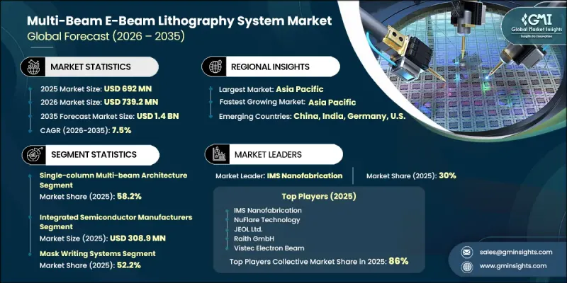
The Global Multi-Beam E-Beam Lithography System Market was valued at USD 692 million in 2025 and is estimated to grow at a CAGR of 7.5% to reach USD 1.4 billion by 2035.
The multi-beam e-beam lithography system industry is advancing steadily as semiconductor manufacturing moves toward increasingly complex designs and tighter precision requirements. Demand for advanced mask writing solutions is growing due to the transition to next-generation chip architectures and the rising need for high-resolution patterning. The increasing complexity of semiconductors used in artificial intelligence and data-centric computing environments is further intensifying the requirement for highly accurate lithography tools. At the same time, the shift toward extreme ultraviolet photomasks is driving adoption of systems capable of delivering superior precision and throughput. Ongoing investments in fabrication facilities worldwide and the expansion of advanced memory technologies are also supporting market growth. These factors collectively highlight the critical role of multi-beam systems in meeting evolving semiconductor production standards while ensuring efficiency, scalability, and performance improvements.
| Market Scope | |
|---|---|
| Start Year | 2025 |
| Forecast Year | 2026-2035 |
| Start Value | $692 Million |
| Forecast Value | $1.4 Billion |
| CAGR | 7.5% |
Growth in the multi-beam e-beam lithography system market is closely linked to the ongoing transition toward advanced semiconductor nodes that demand faster processing, higher accuracy, and improved throughput in mask writing operations. As chipmakers continue to develop more sophisticated logic and memory devices, manufacturing complexity continues to rise, increasing reliance on advanced lithography solutions. The rapid development of processors designed for data-intensive workloads is also contributing to demand, as these applications require intricate and densely packed circuit patterns. This growing complexity is driving the adoption of high-resolution, high-throughput systems capable of supporting next-generation semiconductor designs.
The single-column multi-beam architecture segment accounted for 58.2% share in 2025, supported by its ability to deliver consistent precision and stable performance in mask writing processes. Its compatibility with established workflows and its reliability in handling advanced semiconductor applications contribute to its continued leadership. These systems enable uniform resolution and dependable processing outcomes, making them a preferred choice for high-volume manufacturing environments.
The integrated semiconductor manufacturers segment reached USD 308.9 million in 2025. This dominance is attributed to the extensive production capabilities of these organizations and their continuous requirement for advanced photomasks to support cutting-edge semiconductor development. Their focus on maintaining high standards of accuracy, throughput, and pattern consistency ensures sustained demand for advanced lithography systems.
North America Multi-Beam E-Beam Lithography System Market accounted for 28.5% share in 2025. The region is experiencing steady expansion as semiconductor manufacturers increase adoption of advanced lithography technologies, including EUV-based processes, to support next-generation production requirements. Rising demand for high-performance computing and advanced semiconductor applications across regional markets is further strengthening the need for precise and high-complexity patterning solutions. These dynamics continue to reinforce the importance of multi-beam lithography systems in the region's semiconductor ecosystem.
Key companies operating in the Global Multi-Beam E-Beam Lithography System Market include IMS Nanofabrication, ASML Holding, NuFlare Technology, JEOL Ltd., Vistec Electron Beam GmbH, Raith GmbH, Advantest Corporation, Canon Inc., Hitachi High-Tech Corporation, Elionix Inc., Mapper Lithography, KLA Corporation, Applied Materials, and Toppan Photomasks. Companies in the multi-beam e-beam lithography system market are focusing on strengthening their competitive position through continuous technological advancement and strategic collaborations. Significant investments are being made to enhance system precision, throughput, and scalability to meet evolving semiconductor manufacturing requirements. Organizations are prioritizing research and development to support next-generation lithography innovations and improve writing efficiency. Partnerships with semiconductor manufacturers are enabling better alignment with industry needs and faster adoption of advanced solutions. Companies are also expanding their global presence by increasing production capabilities and targeting emerging semiconductor hubs.
Table of Contents
Chapter 1 Methodology and Scope
- 1.1 Market scope and definition
- 1.2 Research design
- 1.2.1 Research approach
- 1.2.2 Data collection methods
- 1.3 Data mining sources
- 1.3.1 Global
- 1.3.2 Regional/Country
- 1.4 Base estimates and calculations
- 1.4.1 Base year calculation
- 1.4.2 Key trends for market estimation
- 1.5 Primary research and validation
- 1.5.1 Primary sources
- 1.6 Forecast model
- 1.7 Research assumptions and limitations
Chapter 2 Executive Summary
- 2.1 Industry 360° synopsis, 2022 - 2035
- 2.2 Key market trends
- 2.2.1 System architecture trends
- 2.2.2 End-user industry trends
- 2.2.3 Application trends
- 2.2.4 Regional trends
- 2.3 TAM Analysis, 2026-2035
- 2.4 CXO perspectives: Strategic imperatives
Chapter 3 Industry Insights
- 3.1 Industry ecosystem analysis
- 3.1.1 Supplier Landscape
- 3.1.2 Profit Margin
- 3.1.3 Cost structure
- 3.1.4 Value addition at each stage
- 3.1.5 Factor affecting the value chain
- 3.1.6 Disruptions
- 3.2 Industry impact forces
- 3.2.1 Growth drivers
- 3.2.1.1 Demand for more advanced chip manufacturing
- 3.2.1.2 Growth of high-performance computing and AI chips
- 3.2.1.3 Increasing use of EUV and high-NA EUV technology
- 3.2.1.4 Rising investments in new semiconductor fabs worldwide
- 3.2.1.5 More complex memory technologies requiring accurate mask patterns
- 3.2.2 Industry pitfalls and challenges
- 3.2.2.1 High capital cost and operational complexity of multi-beam systems
- 3.2.2.2 Data processing and throughput limitations associated with increasing mask complexity
- 3.2.3 Market opportunities
- 3.2.3.1 Rising adoption of maskless lithography for advanced packaging and specialty devices
- 3.2.3.2 Expansion of advanced packaging driving demand for high-precision patterning
- 3.2.1 Growth drivers
- 3.3 Growth potential analysis
- 3.4 Regulatory landscape
- 3.4.1 North America
- 3.4.2 Europe
- 3.4.3 Asia Pacific
- 3.4.4 Latin America
- 3.4.5 Middle East & Africa
- 3.5 Porter's analysis
- 3.6 PESTEL analysis
- 3.7 Technology and Innovation landscape
- 3.7.1 Current technological trends
- 3.7.2 Emerging technologies
- 3.8 Price trends
- 3.8.1 By region
- 3.8.2 By product
- 3.9 Pricing Strategies
- 3.10 Emerging Business Models
- 3.11 Compliance Requirements
- 3.12 Patent and IP analysis
Chapter 4 Competitive Landscape, 2025
- 4.1 Introduction
- 4.2 Company market share analysis
- 4.2.1 By region
- 4.2.1.1 North America
- 4.2.1.2 Europe
- 4.2.1.3 Asia Pacific
- 4.2.1.4 Latin America
- 4.2.1.5 Middle East & Africa
- 4.2.2 Market concentration analysis
- 4.2.1 By region
- 4.3 Competitive benchmarking of key players
- 4.3.1 Financial performance comparison
- 4.3.1.1 Revenue
- 4.3.1.2 Profit margin
- 4.3.1.3 R&D
- 4.3.2 Product portfolio comparison
- 4.3.2.1 Product range breadth
- 4.3.2.2 Technology
- 4.3.2.3 Innovation
- 4.3.3 Geographic presence comparison
- 4.3.3.1 Global footprint analysis
- 4.3.3.2 Service network coverage
- 4.3.3.3 Market penetration by region
- 4.3.4 Competitive positioning matrix
- 4.3.4.1 Leaders
- 4.3.4.2 Challengers
- 4.3.4.3 Followers
- 4.3.4.4 Niche players
- 4.3.5 Strategic outlook matrix
- 4.3.1 Financial performance comparison
- 4.4 Key developments
- 4.4.1 Mergers and acquisitions
- 4.4.2 Partnerships and collaborations
- 4.4.3 Technological advancements
- 4.4.4 Expansion and investment strategies
- 4.4.5 Digital transformation initiatives
- 4.5 Emerging/ startup competitors landscape
Chapter 5 Market Estimates and Forecast, By System Architecture, 2022 - 2035 (USD Million)
- 5.1 Key trends
- 5.2 Multi-column architecture
- 5.2.1 High-throughput multi-column systems (>10 columns)
- 5.2.2 Mid-range multi-column systems (5-10 columns)
- 5.2.3 Low-column multi-beam systems (<5 columns)
- 5.3 Single-column multi-beam architecture
- 5.3.1 High-beam-count systems (>10,000 beams)
- 5.3.2 Mid-beam-count systems (1,000-10,000 beams)
Chapter 6 Market Estimates and Forecast, By End-User Industry, 2022 - 2035 (USD Million)
- 6.1 Key trends
- 6.2 Integrated semiconductor manufacturers
- 6.3 Independent photomask shops
- 6.4 Academic & research institutions
Chapter 7 Market Estimates and Forecast, By Application, 2022 - 2035 (USD Million)
- 7.1 Key trends
- 7.2 Mask writing systems
- 7.3 Direct wafer writing systems
Chapter 8 Market Estimates and Forecast, By Region, 2022 - 2035 (USD Million)
- 8.1 Key trends
- 8.2 North America
- 8.2.1 U.S.
- 8.2.2 Canada
- 8.3 Europe
- 8.3.1 Germany
- 8.3.2 UK
- 8.3.3 France
- 8.3.4 Spain
- 8.3.5 Italy
- 8.3.6 Russia
- 8.4 Asia Pacific
- 8.4.1 China
- 8.4.2 India
- 8.4.3 Japan
- 8.4.4 Australia
- 8.4.5 South Korea
- 8.5 Latin America
- 8.5.1 Brazil
- 8.5.2 Mexico
- 8.5.3 Argentina
- 8.6 Middle East and Africa
- 8.6.1 South Africa
- 8.6.2 Saudi Arabia
- 8.6.3 UAE
Chapter 9 Company Profiles
- 9.1 Global Key Players
- 9.1.1 IMS Nanofabrication
- 9.1.2 NuFlare Technology
- 9.1.3 JEOL Ltd.
- 9.1.4 Raith GmbH
- 9.1.5 Vistec Electron Beam
- 9.2 Regional key players
- 9.2.1 North America
- 9.2.1.1 KLA Corporation
- 9.2.1.2 Applied Materials
- 9.2.2 Asia Pacific
- 9.2.2.1 Advantest Corporation
- 9.2.2.2 Canon Inc.
- 9.2.2.3 Hitachi High-Tech Corporation
- 9.2.2.4 Elionix Inc.
- 9.2.2.5 Toppan Photomasks
- 9.2.3 Europe
- 9.2.3.1 ASML Holding
- 9.2.3.2 Mapper Lithography
- 9.2.1 North America

