
PUBLISHER: Information Network | PRODUCT CODE: 1479763

PUBLISHER: Information Network | PRODUCT CODE: 1479763
Sub-100nm Lithography: Market Analysis and Strategic Issues
Driving Forces
As semiconductor technology nodes shrink and demand for smaller and more complex semiconductor devices increases, several driving forces push the advancement of lithography technology to meet these challenges:
Technological Scaling: With each new technology node, semiconductor manufacturers aim to reduce the size of transistors and interconnects to improve performance, power efficiency, and density. Advanced lithography techniques are essential for patterning these smaller features with high precision and resolution, driving the development of next-generation lithography tools.
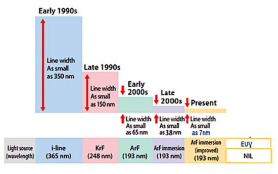
EUV Lithography Adoption: Extreme ultraviolet (EUV) lithography has emerged as a leading candidate for patterning critical layers in advanced semiconductor manufacturing processes. EUV offers shorter wavelengths than traditional optical lithography, enabling the fabrication of smaller feature sizes and more complex patterns. As nodes get smaller, the adoption of EUV lithography becomes increasingly necessary to achieve the required patterning resolution.
Multi-Patterning Techniques: As feature sizes approach the limits of optical lithography, multipatterning techniques such as self-aligned double patterning (SADP), self-aligned quadruple patterning (SAQP), and multi-beam maskless lithography (MBML) become indispensable for achieving the desired feature density and pitch. These techniques involve multiple exposure and etching steps to create intricate patterns, driving the need for advanced lithography solutions.
Resolution Enhancement Technologies (RET): To improve the resolution and fidelity of pattern transfer, lithography tools incorporate resolution enhancement techniques such as optical proximity correction (OPC), phase-shift masks (PSM), and source mask optimization (SMO). These RETs help mitigate the effects of diffraction and other optical limitations, enabling the fabrication of finer features at advanced nodes.
Process Control and Yield Improvement: As feature sizes shrink, maintaining tight process control becomes increasingly challenging. Advanced lithography tools incorporate sophisticated metrology and process control capabilities to ensure uniformity, overlay accuracy, and defect reduction. These capabilities are essential for achieving high yields and manufacturing consistency at advanced nodes.
Emerging Applications and Market Demand: Emerging technologies such as artificial intelligence (AI), 5G connectivity, autonomous vehicles, and IoT devices drive the demand for specialized semiconductor devices with specific performance requirements. Advanced lithography solutions are essential for patterning the complex structures and materials required for these applications, driving innovation in lithography technology.
The Need for This Report
Semiconductor lithography stands as a cornerstone in the realm of semiconductor manufacturing, serving as a pivotal process in the creation of intricate semiconductor devices that power modern electronics. As semiconductor technology advances, lithography techniques evolve in tandem, pushing the boundaries of resolution, precision, and throughput to enable the fabrication of ever-smaller and more complex semiconductor structures. This comprehensive report delves into the multifaceted landscape of semiconductor lithography, exploring key technologies, market trends, industry challenges, and future prospects shaping the semiconductor lithography ecosystem.
The semiconductor industry is witnessing a relentless pursuit of miniaturization, driven by the demand for higher-performance and more energy-efficient electronic devices. As feature sizes shrink to nanoscale dimensions, lithography emerges as a critical enabler, allowing semiconductor manufacturers to pattern intricate circuit designs with unparalleled precision. Advanced lithography techniques such as extreme ultraviolet (EUV) lithography, multiple patterning, and immersion lithography play pivotal roles in achieving sub-10 nanometer feature sizes, pushing the limits of semiconductor manufacturing capabilities.
In addition to technological advancements, the semiconductor lithography market is influenced by a myriad of factors, including market dynamics, regulatory policies, and industry collaborations. This report provides a comprehensive analysis of the global semiconductor lithography market, offering insights into market size, growth drivers, competitive landscape, and emerging opportunities. Through a detailed examination of lithography equipment, materials, and processes, stakeholders gain a deeper understanding of the evolving semiconductor lithography landscape and its impact on the semiconductor industry.
Furthermore, the report explores key challenges and bottlenecks facing semiconductor lithography, ranging from mask complexity and defect reduction to cost constraints and yield optimization. By identifying critical issues and potential solutions, stakeholders can devise strategies to mitigate risks and capitalize on growth opportunities in the semiconductor lithography market.
As semiconductor lithography continues to evolve in response to technological advancements and market demands, stakeholders across the semiconductor ecosystem must stay abreast of the latest developments and trends shaping the industry. This report serves as a valuable resource for semiconductor manufacturers, equipment suppliers, investors, and other industry participants seeking actionable insights into the dynamic landscape of semiconductor lithography. Through comprehensive analysis and strategic recommendations, this report empowers stakeholders to navigate the complex terrain of semiconductor lithography and drive innovation in semiconductor manufacturing.
Report Coverage
This report provides a detailed analysis of the global semiconductor lithography market, including historical data, current market size, and projected growth trends. It may also include market segmentation based on technology, end-user industry, and geographical regions.
It explores the various lithography technologies utilized in semiconductor manufacturing, such as optical lithography, extreme ultraviolet (EUV) lithography, multiple patterning, nanoimprint lithography, and others. This section delves into the principles, advancements, and applications of each technology.
Market Segmentation: Unit and Revenue segments the semiconductor lithography market based on technology types are forecast by:
|
|
The report provides insights into market share of lithography vendors by equipment type including revenue and unit shipments. Market shares by vendor are provided since 1992. The report identifies and analyzes current and emerging trends driving the semiconductor lithography market, such as node migration, China sanctions, and new semiconductor materials, particularly silicon carbide.
Table of Contents
Chapter 1. Introduction
- 1.1. The Need For This Report
Chapter 2. Executive Summary
- 2.1. Summary of Major Issues
- 2.2. Summary of Market Opportunities
Chapter 3. Lithography Issues And Trends
- 3.1. Optical Systems
- 3.1.1. Introduction
- 3.1.2. Step-and-Repeat Aligners
- 3.1.3. Deep Ultraviolet (DUV)
- 3.2. EUV
- 3.5. Nano-Imprint Lithography
- 3.4. X-Ray Lithography
- 3.3. Electron Beam Lithography
- 3.4. Ion Beam Lithography
Chapter 4. User - Supplier Strategies
- 4.1. Determining Lithography Needs
- 4.2. Benchmarking a Vendor
- 4.2.1. Pricing
- 4.2.2. Vendor Commitment and Attitudes
- 4.2.3. Vendor Capabilities
- 4.2.4. System Capabilities
- 4.2.5. Vendor Feedback During Equipment Evaluation
- 4.2.6. Vendor Feedback During Device Production
- 4.3. Competitive Environment
- 4.4. Equipment For Class 1 Cleanrooms
- 4.5. Equipment For the Factory of the Future
- 4.6. Opportunities
Chapter 5. Market Forecast
- 5.1. Driving Forces
- 5.1.1. Technical Trends
- 5.1.2. Economic Trends
- 5.1.3. Optical Limitations
- 5.2. Market Forecast Assumptions
- 5.3. Market Forecast
List of Tables
- 3.1. Wavelength "Generations"
- 3.2. Characteristics of X-Ray Systems
- 5.1. Worldwide Capital Spending
- 5.2. DRAM Lithographic Requirements
- 5.3. Worldwide Optical Stepper Market
- 5.4. Worldwide Stepper Market Shares
List of Figures
- 1.1. Lithographic Equipment Requirements for DRAMs
- 3.1. Lithography Options For MPUs/DRAMs
- 3.2. Lithography Options For Flash
- 3.3. Illustration of Stepper Exposure System
- 3.4. Lens Arrangement For Submicron Features
- 3.5. Excimer Laser Evolution
- 3.6. EUV Lithography
- 3.7. Thermoplastic Nanoimprint Lithography Process
- 3.8. Step And Flash Nanoimprint Lithography Process
- 3.9. Illustration of X-Ray Lithography
- 3.10. Schematic Of Scalpel Electron Beam System
- 3.11. Multi-Source E-Beam Lithography
- 3.12. Ion Projection Lithography System
- 4.1. Manufacturing Costs Per Exposure Station
- 5.1. Lithography Market Vs Equipment Market
- 5.2. Lithography Double Exposure Technique
- 5.3. Lithography Requirements
- 5.4. Lithography Extensions
- 5.5. Lithography Cost of Ownership
- 5.6. Segmentation of Stepper/Scan Shipments
- 5.7. Market Shares of Vendors (Units)
- 5.8. Unit Market Shares of Vendors
- 5.9. Worldwide I-Line Market Shares
- 5.10. Worldwide 248nm Market Shares
- 5.11. Worldwide 193nm Dry Market Shares
- 5.12. Worldwide 193nm Wet Market Shares
- 5.13. Market Shares of Vendors (Revenues)

