
PUBLISHER: MarketsandMarkets | PRODUCT CODE: 1881221
PUBLISHER: MarketsandMarkets | PRODUCT CODE: 1881221
Semiconductor Ceramic Packaging Materials Market by Material, Packaging Technology, End-use Industry, & Region - Global Forecast to 2030
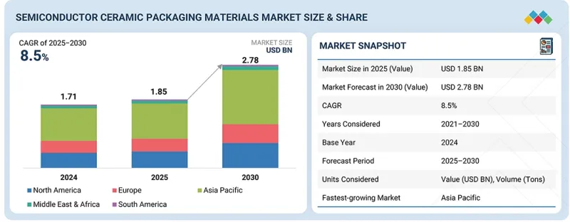
The semiconductor ceramic packaging materials market size is projected to grow from USD 1.85 billion in 2025 to USD 2.78 billion by 2030, registering a CAGR of 8.5% during the forecast period.
| Scope of the Report | |
|---|---|
| Years Considered for the Study | 2021-2030 |
| Base Year | 2024 |
| Forecast Period | 2025-2030 |
| Units Considered | Value (USD Million/Billion), Volume (Tons) |
| Segments | Material, Packaging Technology, End-use Industry, and Region |
| Regions covered | Asia Pacific, North America, Europe, the Middle East & Africa, and South America |
The demand for semiconductor ceramic packaging materials is increasing due to the growing complexity and miniaturization of modern electronic devices, which require packaging that can reliably manage heat and maintain signal integrity. Rising adoption of high-power and high-frequency applications, such as electric vehicles, industrial automation, and advanced medical devices, is driving the need for materials with superior thermal conductivity and mechanical strength.
Additionally, the shift toward high-density multi-chip modules and system-in-package designs requires ceramics that can support precise assembly and long-term reliability. Increasing environmental and regulatory requirements for non-toxic, durable, and stable materials also favor ceramics over traditional packaging. These combined technological, industrial, and regulatory pressures are collectively fueling sustained growth in market demand.
"By material, the alumina segment is anticipated to account for the largest market share during the forecast period"
Alumina accounts for the largest share in the semiconductor ceramic packaging materials market due to its proven reliability, versatility, and cost-effectiveness across a wide range of applications. Its combination of good thermal conductivity, excellent electrical insulation, and high mechanical strength allows it to meet the performance requirements of both low- and high-power semiconductor devices. Alumina is compatible with established manufacturing processes, including co-firing and metallization techniques, enabling scalable production with minimal defects. Its widespread availability and relatively lower raw material cost compared to other materials make it a preferred choice for mass-market applications. Additionally, alumina's stability under thermal cycling and harsh environmental conditions ensures long-term device performance, reinforcing its dominant position in the market.
"By end-use industry, the consumer electronics segment is anticipated to account for the largest market share during the forecast period"
Consumer electronics account for the largest share of the semiconductor ceramic packaging materials market because the sector drives high-volume demand for reliable and durable semiconductor components. Rapid growth in global electronics consumption, including smartphones, laptops, tablets, audio devices, and wearable technology, increases the need for packaging materials that can maintain performance under frequent use and varying environmental conditions. Manufacturers prioritize components that ensure long-term stability and minimize device failure, supporting brand reputation and customer satisfaction. The wide variety of products and continuous technological upgrades in this industry, including advanced displays, processing power, and connectivity features, make consumer electronics the primary driver of ceramic packaging material demand.
"By packaging technology, the surface mount packages - leadless segment is anticipated to account for the largest market share during the forecast period"
Surface mount packages- leadless account for the largest share in the semiconductor ceramic packaging materials market because they allow for more precise and efficient assembly of semiconductor devices compared to traditional through-hole methods. This technology supports higher component density on printed circuit boards, enabling compact designs and improved signal integrity in advanced electronics. It also enhances mechanical stability and reduces the risk of solder joint failures, which is critical for applications in automotive, aerospace, and high-performance computing. Additionally, leadless surface mount technology is compatible with automated manufacturing and inspection processes, improving production speed and consistency. Its ability to support miniaturization, high-frequency operation, and reliable thermal management makes this packaging technology the preferred choice for modern semiconductor applications, driving its growth in the market.
"Asia Pacific is anticipated to account for the largest market share during the forecast period"
Asia Pacific holds the largest share in the semiconductor ceramic packaging materials market because the region is a global hub for semiconductor assembly, testing, and packaging operations. Strong investments in research and development of advanced packaging technologies drive demand for high-performance ceramic materials. The concentration of electronics manufacturing clusters in countries like China, Taiwan, and South Korea enables efficient production and rapid adoption of new packaging solutions. Additionally, the growing presence of international semiconductor companies establishing regional operations and partnerships increases the consumption of ceramic materials. Supportive industrial policies, export-oriented production, and rising domestic demand for advanced electronics further strengthen the region's market dominance.
In-depth interviews were conducted with chief executive officers (CEOs), marketing directors, other innovation and technology directors, and executives from various key organizations operating in the semiconductor ceramic packaging materials market, and information was gathered from secondary research to determine and verify the market size of several segments.
- By Company Type: Tier 1 - 50%, Tier 2 - 30%, and Tier 3 - 20%
- By Designation: Managers- 15%, Directors - 20%, and Others - 65%
- By Region: North America - 30%, Europe - 25%, Asia Pacific - 35%, the Middle East & Africa -5%, and South America- 5%
The semiconductor ceramic packaging materials market comprises major KYOCERA Corporation (Japan), CeramTec GmbH (Germany), CoorsTek (US), Materion Corporation (US), Resonac Holdings Corporation (Japan), NGK INSULATORS, LTD. (Japan), AGC Inc. (Japan), Morgan Advanced Materials (UK), MARUWA Co., Ltd. (Japan), and Tokuyama Corporation (Japan). The study includes an in-depth competitive analysis of these key players in the semiconductor ceramic packaging materials market, with their company profiles, recent developments, and key market strategies.
Research Coverage
This report segments the semiconductor ceramic packaging materials market on the basis of material, packaging technology, end-use industry, and region, and provides estimations for the overall value of the market across various regions. A detailed analysis of key industry players has been conducted to provide insights into their business overviews, products & services, key strategies, and expansions associated with the semiconductor ceramic packaging materials market.
Key Benefits of Buying This Report
This research report is focused on various levels of analysis - industry analysis (industry trends), market ranking analysis of top players, and company profiles, which together provide an overall view of the competitive landscape; emerging and high-growth segments of the semiconductor ceramic packaging materials market; high-growth regions; and market drivers, restraints, opportunities, and challenges.
The report provides insights on the following pointers:
- Analysis of drivers (expansion of automotive electronics and EV power modules boosting ceramic packaging adoption), restraints (high cost of ceramic packaging materials compared to polymer or metal-based packaging), opportunities (regional localization of semiconductor manufacturing encouraging investment), and challenges (limited design flexibility of ceramic materials makes fabricating complex geometries challenging) influencing the growth of semiconductor ceramic packaging materials market.
- Market Penetration: Comprehensive information on the semiconductor ceramic packaging materials offered by top players in the global semiconductor ceramic packaging materials market.
- Product Development/Innovation: Detailed insights on upcoming technologies, expansions, and partnerships in the semiconductor ceramic packaging materials market.
- Market Development: Comprehensive information about lucrative emerging markets, the report analyzes the markets for semiconductor ceramic packaging materials market across regions.
- Market Capacity: Production capacity of the companies is provided wherever available with upcoming capacities for the semiconductor ceramic packaging materials market.
- Competitive Assessment: In-depth assessment of market shares, strategies, products, and manufacturing capabilities of leading players in the semiconductor ceramic packaging materials market.
TABLE OF CONTENTS
1 INTRODUCTION
- 1.1 STUDY OBJECTIVES
- 1.2 MARKET DEFINITION
- 1.3 STUDY SCOPE
- 1.3.1 MARKETS COVERED
- 1.3.2 INCLUSIONS & EXCLUSIONS
- 1.3.3 YEARS CONSIDERED
- 1.3.4 CURRENCY CONSIDERED
- 1.3.5 UNITS CONSIDERED
- 1.4 LIMITATIONS
- 1.5 STAKEHOLDERS
2 RESEARCH METHODOLOGY
- 2.1 RESEARCH DATA
- 2.1.1 SECONDARY DATA
- 2.1.1.1 Key data from secondary sources
- 2.1.2 PRIMARY DATA
- 2.1.2.1 Key data from primary sources
- 2.1.2.2 Key primary sources
- 2.1.2.3 Key players for primary interviews
- 2.1.2.4 Breakdown of interviews with experts
- 2.1.2.5 Key industry insights
- 2.1.1 SECONDARY DATA
- 2.2 BASE NUMBER CALCULATION
- 2.2.1 SUPPLY-SIDE ANALYSIS
- 2.2.2 DEMAND-SIDE ANALYSIS
- 2.3 GROWTH FORECAST
- 2.3.1 SUPPLY SIDE
- 2.3.2 DEMAND SIDE
- 2.4 MARKET SIZE ESTIMATION
- 2.4.1 BOTTOM-UP APPROACH
- 2.4.2 TOP-DOWN APPROACH
- 2.5 DATA TRIANGULATION
- 2.6 RESEARCH ASSUMPTION
- 2.7 GROWTH FORECAST
- 2.8 RISK ASSESSMENT
- 2.9 FACTOR ANALYSIS
3 EXECUTIVE SUMMARY
4 PREMIUM INSIGHTS
- 4.1 ATTRACTIVE OPPORTUNITIES FOR PLAYERS IN SEMICONDUCTOR CERAMIC PACKAGING MATERIALS MARKET
- 4.2 SEMICONDUCTOR CERAMIC PACKAGING MATERIALS MARKET, BY MATERIAL
- 4.3 SEMICONDUCTOR CERAMIC PACKAGING MATERIALS MARKET, BY PACKAGING TECHNOLOGY
- 4.4 SEMICONDUCTOR CERAMIC PACKAGING MATERIALS MARKET, BY END-USE INDUSTRY
- 4.5 SEMICONDUCTOR CERAMIC PACKAGING MATERIALS MARKET, BY COUNTRY
5 MARKET OVERVIEW
- 5.1 INTRODUCTION
- 5.2 MARKET DYNAMICS
- 5.2.1 DRIVERS
- 5.2.1.1 Expansion of automotive electronics and EV power modules
- 5.2.1.2 Growth in 5G infrastructure and RF devices
- 5.2.2 RESTRAINTS
- 5.2.2.1 Higher cost of ceramic packaging materials than polymer or metal-based packaging
- 5.2.3 OPPORTUNITIES
- 5.2.3.1 Regional localization of semiconductor manufacturing encouraging investment
- 5.2.3.2 Advanced multilayer ceramic materials for emerging 2.5D/ 3D semiconductor packaging
- 5.2.4 CHALLENGES
- 5.2.4.1 Difficulty in bonding to dissimilar materials
- 5.2.4.2 Limited design flexibility makes fabricating complex geometries challenging
- 5.2.1 DRIVERS
- 5.3 GENERATIVE AI
- 5.3.1 INTRODUCTION
- 5.4 IMPACT ON SEMICONDUCTOR CERAMIC PACKAGING MATERIALS MARKET
6 INDUSTRY TRENDS
- 6.1 INTRODUCTION
- 6.2 TRENDS/DISRUPTIONS IMPACTING CUSTOMER BUSINESS
- 6.3 SUPPLY CHAIN ANALYSIS
- 6.4 IMPACT OF 2025 US TARIFF -SEMICONDUCTOR CERAMIC PACKAGING MATERIALS MARKET
- 6.4.1 INTRODUCTION
- 6.4.2 KEY TARIFF RATES
- 6.4.3 PRICE IMPACT ANALYSIS
- 6.4.4 IMPACT ON REGION
- 6.4.4.1 North America
- 6.4.4.2 Europe
- 6.4.4.3 Asia Pacific
- 6.4.5 IMPACT ON END-USE INDUSTRY
- 6.5 INVESTMENT LANDSCAPE AND FUNDING SCENARIO
- 6.6 PRICING ANALYSIS
- 6.6.1 AVERAGE SELLING PRICE TREND OF SEMICONDUCTOR CERAMIC PACKAGING MATERIALS MARKET, BY REGION, 2021-2024
- 6.6.2 AVERAGE SELLING PRICE TREND OF SEMICONDUCTOR CERAMIC PACKAGING MATERIALS MARKET, BY MATERIAL, 2021-2024
- 6.6.3 AVERAGE SELLING PRICE TREND OF SEMICONDUCTOR CERAMIC PACKAGING MATERIALS, BY KEY PLAYER, 2024
- 6.7 ECOSYSTEM ANALYSIS
- 6.8 TECHNOLOGY ANALYSIS
- 6.8.1 KEY TECHNOLOGIES
- 6.8.2 COMPLEMENTARY TECHNOLOGIES
- 6.8.3 ADJACENT TECHNOLOGIES
- 6.9 PATENT ANALYSIS
- 6.9.1 METHODOLOGY
- 6.9.2 PATENTS GRANTED WORLDWIDE, 2015-2024
- 6.9.2.1 Patent publication trends
- 6.9.3 INSIGHTS
- 6.9.4 LEGAL STATUS OF PATENTS
- 6.9.5 JURISDICTION ANALYSIS
- 6.9.6 TOP APPLICANTS
- 6.9.7 LIST OF MAJOR PATENTS
- 6.10 TRADE ANALYSIS
- 6.10.1 IMPORT SCENARIO (HS CODE 85419000)
- 6.10.2 EXPORT SCENARIO (HS CODE 85419000)
- 6.11 KEY CONFERENCES AND EVENTS, 2026-2027
- 6.12 TARIFF AND REGULATORY LANDSCAPE
- 6.12.1 TARIFF ANALYSIS
- 6.13 STANDARDS AND REGULATORY LANDSCAPE
- 6.13.1 REGULATORY BODIES, GOVERNMENT AGENCIES, AND OTHER ORGANIZATIONS
- 6.13.2 STANDARDS
- 6.14 PORTER'S FIVE FORCES ANALYSIS
- 6.14.1 THREAT OF NEW ENTRANTS
- 6.14.2 THREAT OF SUBSTITUTES
- 6.14.3 BARGAINING POWER OF SUPPLIERS
- 6.14.4 BARGAINING POWER OF BUYERS
- 6.14.5 INTENSITY OF COMPETITIVE RIVALRY
- 6.15 KEY STAKEHOLDERS AND BUYING CRITERIA
- 6.15.1 KEY STAKEHOLDERS IN BUYING PROCESS
- 6.15.2 BUYING CRITERIA
- 6.16 MACROECONOMIC OUTLOOK
- 6.16.1 GDP TRENDS AND FORECASTS OF MAJOR ECONOMIES
- 6.17 CASE STUDY ANALYSIS
- 6.17.1 LOW THERMAL RESISTANCE PACKAGING FOR HIGH POWER ELECTRONICS
- 6.17.2 EFFECTS OF BETA-SI3N4 SEEDS ON MICROSTRUCTURE AND PERFORMANCE OF SI3N4 CERAMICS IN SEMICONDUCTOR PACKAGE
- 6.17.3 PREPARATION OF DIAMOND FILM SUBSTRATES ON ALN CERAMIC AND THEIR PERFORMANCE IN LED PACKAGING
7 SEMICONDUCTOR CERAMIC PACKAGING MATERIALS MARKET, BY MATERIAL
- 7.1 INTRODUCTION
- 7.2 ALUMINA
- 7.2.1 HIGH-TEMPERATURE PERFORMANCE IN SEMICONDUCTOR DEVICES TO DRIVE DEMAND
- 7.3 ALUMINUM NITRIDE
- 7.3.1 SUPERIOR THERMAL AND ELECTRICAL PROPERTIES TO DRIVE MARKET
- 7.4 SILICON NITRIDE
- 7.4.1 HIGH MECHANICAL STRENGTH AND THERMAL SHOCK RESILIENCE TO DRIVE DEMAND
- 7.5 SILICON CARBIDE
- 7.5.1 MATERIAL ADVANCEMENTS TO DRIVE HIGH DENSITY AND THERMALLY STABLE CHIP PACKAGING
- 7.6 BERYLLIUM OXIDE
- 7.6.1 EFFICIENT HEAT DISSIPATION TO DRIVE NEXT-GENERATION HIGH-POWER PACKAGE DESIGNS
- 7.7 OTHER MATERIALS
- 7.7.1 BORON NITRIDE
- 7.7.2 ZIRCONIA
8 SEMICONDUCTOR CERAMIC PACKAGING MATERIALS MARKET, BY PACKAGING TECHNOLOGY
- 8.1 INTRODUCTION
- 8.2 THROUGH-HOLE PACKAGES
- 8.2.1 ENHANCED DEVICE DURABILITY AND THERMAL PERFORMANCE TO DRIVE DEMAND
- 8.3 SURFACE MOUNT PACKAGES - LEADED
- 8.3.1 EFFICIENT ASSEMBLY AND RELIABLE PERFORMANCE TO DRIVE DEMAND
- 8.4 SURFACE MOUNT PACKAGES - LEADLESS
- 8.4.1 SUPERIOR ELECTRICAL PERFORMANCE AND EFFICIENT MANUFACTURING TO DRIVE DEMAND
- 8.5 ADVANCED MINIATURIZED PACKAGES
- 8.5.1 HIGH-PERFORMANCE INTEGRATION AND EFFICIENT CONNECTIVITY TO DRIVE MARKET
- 8.6 OTHER PACKAGING TECHNOLOGIES
- 8.6.1 FLIP-CHIP CERAMIC PACKAGES
- 8.6.2 MULTI-CHIP MODULES
9 SEMICONDUCTOR CERAMIC PACKAGING MATERIALS MARKET, BY END-USE INDUSTRY
- 9.1 INTRODUCTION
- 9.2 CONSUMER ELECTRONICS
- 9.2.1 INCREASE IN ADVANCED CERAMIC PACKAGING ADOPTION FOR HIGH-PERFORMANCE, RELIABLE DEVICES
- 9.3 AUTOMOTIVE
- 9.3.1 RISE IN VEHICLE PRODUCTION TO DRIVE MARKET
- 9.4 HEALTHCARE
- 9.4.1 EXPANSION OF HEALTHCARE MARKETS TO DRIVE DEMAND FOR HIGH-PERFORMANCE PACKAGING MATERIALS
- 9.5 IT & TELECOMMUNICATION
- 9.5.1 5G AND DIGITAL INFRASTRUCTURE EXPANSION TO DRIVE DEMAND
- 9.6 AEROSPACE & DEFENSE
- 9.6.1 NEXT-GENERATION AEROSPACE TECHNOLOGIES TO DRIVE HIGH-PERFORMANCE PACKAGING ADOPTION
- 9.7 OTHER END-USE INDUSTRIES
- 9.7.1 RAIL & TRANSPORTATION
- 9.7.2 RENEWABLE ENERGY
10 SEMICONDUCTOR CERAMIC PACKAGING MATERIALS MARKET, BY REGION
- 10.1 INTRODUCTION
- 10.2 ASIA PACIFIC
- 10.2.1 CHINA
- 10.2.1.1 Rapid growth of 5G infrastructure and consumer electronics market
- 10.2.2 JAPAN
- 10.2.2.1 Continuous investment in R&D for semiconductor packaging materials
- 10.2.3 INDIA
- 10.2.3.1 Government incentives through India Semiconductor Mission
- 10.2.4 SOUTH KOREA
- 10.2.4.1 Presence of major semiconductor manufacturers like Samsung and SK hynix
- 10.2.5 TAIWAN
- 10.2.5.1 Leadership in semiconductor manufacturing
- 10.2.6 REST OF ASIA PACIFIC
- 10.2.1 CHINA
- 10.3 NORTH AMERICA
- 10.3.1 US
- 10.3.1.1 Strong semiconductor, aerospace, and defense industries
- 10.3.2 CANADA
- 10.3.2.1 Expansion of technology infrastructure
- 10.3.3 MEXICO
- 10.3.3.1 Emergence as manufacturing hub to drive demand
- 10.3.1 US
- 10.4 EUROPE
- 10.4.1 GERMANY
- 10.4.1.1 Growth in automotive manufacturing and ADAS integration
- 10.4.2 ITALY
- 10.4.2.1 Industrial automation and IoT electronics growth
- 10.4.3 FRANCE
- 10.4.3.1 High investment in medical electronics demanding hermetic ceramic packages
- 10.4.4 UK
- 10.4.4.1 Government initiatives for semiconductor sovereignty
- 10.4.5 SPAIN
- 10.4.5.1 Support for local semiconductor and electronics production
- 10.4.6 REST OF EUROPE
- 10.4.1 GERMANY
- 10.5 MIDDLE EAST & AFRICA
- 10.5.1 GCC COUNTRIES
- 10.5.1.1 Saudi Arabia
- 10.5.1.1.1 Saudi Arabia's Vision 2030 spurs investment
- 10.5.1.2 UAE
- 10.5.1.2.1 National Strategy for Advanced Industries (Operation 300bn)
- 10.5.1.3 Rest of GCC countries
- 10.5.1.4 South Africa
- 10.5.1.4.1 Expansion in automotive component manufacturing
- 10.5.1.5 Rest of Middle East & Africa
- 10.5.1.1 Saudi Arabia
- 10.5.1 GCC COUNTRIES
- 10.6 SOUTH AMERICA
- 10.6.1 ARGENTINA
- 10.6.1.1 Industrial modernization and import substitution
- 10.6.2 BRAZIL
- 10.6.2.1 Growing industrial and consumer electronics production
- 10.6.3 REST OF SOUTH AMERICA
- 10.6.1 ARGENTINA
11 COMPETITIVE LANDSCAPE
- 11.1 INTRODUCTION
- 11.2 KEY PLAYER STRATEGIES/RIGHT TO WIN
- 11.3 MARKET SHARE ANALYSIS, 2024
- 11.4 REVENUE ANALYSIS, 2021-2024
- 11.5 COMPANY EVALUATION MATRIX: KEY PLAYERS, 2024
- 11.5.1 STARS
- 11.5.2 EMERGING LEADERS
- 11.5.3 PERVASIVE PLAYERS
- 11.5.4 PARTICIPANTS
- 11.5.5 COMPANY FOOTPRINT: KEY PLAYERS, 2024
- 11.5.5.1 Company footprint
- 11.5.5.2 Region footprint
- 11.5.5.3 Material footprint
- 11.5.5.4 Packaging technology footprint
- 11.5.5.5 End-use industry footprint
- 11.6 COMPANY EVALUATION MATRIX: STARTUPS/SMES, 2024
- 11.6.1 PROGRESSIVE COMPANIES
- 11.6.2 RESPONSIVE COMPANIES
- 11.6.3 DYNAMIC COMPANIES
- 11.6.4 STARTING BLOCKS
- 11.6.5 COMPETITIVE BENCHMARKING
- 11.6.5.1 Detailed list of key startups/SMEs
- 11.6.5.2 Competitive benchmarking of key startups/SMEs
- 11.7 BRAND/PRODUCT COMPARISON
- 11.8 COMPANY VALUATION AND FINANCIAL METRICS
- 11.9 COMPETITIVE SCENARIO AND TRENDS
- 11.9.1 DEALS
- 11.9.2 EXPANSIONS
- 11.9.3 OTHER DEVELOPMENTS
12 COMPANY PROFILES
- 12.1 KEY PLAYERS
- 12.1.1 KYOCERA CORPORATION
- 12.1.1.1 Business overview
- 12.1.1.2 Products/Solutions/Services offered
- 12.1.1.3 Recent developments
- 12.1.1.3.1 Deals
- 12.1.1.3.2 Expansions
- 12.1.1.4 MnM view
- 12.1.1.4.1 Key strengths
- 12.1.1.4.2 Strategic choices
- 12.1.1.4.3 Weaknesses and competitive threats
- 12.1.2 CERAMTEC GMBH
- 12.1.2.1 Business overview
- 12.1.2.2 Products/Solutions/Services offered
- 12.1.2.3 MnM view
- 12.1.2.3.1 Key strengths
- 12.1.2.3.2 Strategic choices
- 12.1.2.3.3 Weaknesses and competitive threats
- 12.1.3 COORSTEK
- 12.1.3.1 Business overview
- 12.1.3.2 Products/Solutions/Services offered
- 12.1.3.3 Recent developments
- 12.1.3.3.1 Others
- 12.1.3.4 MnM view
- 12.1.3.4.1 Key strengths
- 12.1.3.4.2 Strategic choices
- 12.1.3.4.3 Weaknesses and competitive threats
- 12.1.4 MORGAN ADVANCED MATERIALS
- 12.1.4.1 Business overview
- 12.1.4.2 Products/Solutions/Services offered
- 12.1.4.3 Recent developments
- 12.1.4.3.1 Others
- 12.1.4.4 MnM view
- 12.1.4.4.1 Key strengths
- 12.1.4.4.2 Strategic choices
- 12.1.4.4.3 Weaknesses and competitive threats
- 12.1.5 NGK INSULATORS, LTD.
- 12.1.5.1 Business overview
- 12.1.5.2 Products/Solutions/Services offered
- 12.1.5.3 MnM view
- 12.1.5.3.1 Key strengths
- 12.1.5.3.2 Strategic choices
- 12.1.5.3.3 Weaknesses and competitive threats
- 12.1.6 MARUWA CO., LTD.
- 12.1.6.1 Business overview
- 12.1.6.2 Products/Solutions/Services offered
- 12.1.6.3 MnM view
- 12.1.6.3.1 Key strengths
- 12.1.6.3.2 Strategic choices
- 12.1.6.3.3 Weaknesses and competitive threats
- 12.1.7 AGC INC.
- 12.1.7.1 Business overview
- 12.1.7.2 Products/Solutions/Services offered
- 12.1.7.3 Recent developments
- 12.1.7.3.1 Others
- 12.1.7.4 MnM view
- 12.1.7.4.1 Key strengths
- 12.1.7.4.2 Strategic choices
- 12.1.7.4.3 Weaknesses and competitive threats
- 12.1.8 MATERION CORPORATION
- 12.1.8.1 Business overview
- 12.1.8.2 Products/Solutions/Services offered
- 12.1.8.3 MnM view
- 12.1.8.3.1 Key strengths
- 12.1.8.3.2 Strategic choices
- 12.1.8.3.3 Weaknesses and competitive threats
- 12.1.9 TOKUYAMA CORPORATION
- 12.1.9.1 Business overview
- 12.1.9.2 Products/Solutions/Services offered
- 12.1.9.3 Recent developments
- 12.1.9.3.1 Expansions
- 12.1.9.4 MnM view
- 12.1.9.4.1 Key strengths
- 12.1.9.4.2 Strategic choices
- 12.1.9.4.3 Weaknesses and competitive threats
- 12.1.10 FERROTEC CORPORATION
- 12.1.10.1 Business overview
- 12.1.10.2 Products/Solutions/Services offered
- 12.1.10.3 Recent developments
- 12.1.10.3.1 Expansions
- 12.1.10.4 MnM view
- 12.1.10.4.1 Key strengths
- 12.1.10.4.2 Strategic choices
- 12.1.10.4.3 Weaknesses and competitive threats
- 12.1.1 KYOCERA CORPORATION
- 12.2 OTHER PLAYERS
- 12.2.1 GREAT CERAMIC
- 12.2.2 ADTECH CERAMICS
- 12.2.3 XIAMEN MASCERA TECHNOLOGY CO., LTD.
- 12.2.4 ORTECH, INC.
- 12.2.5 ADVANCED CERAMIC MATERIALS
- 12.2.6 STC MATERIAL SOLUTIONS
- 12.2.7 NISHIMURA ADVANCED CERAMICS CO., LTD.
- 12.2.8 JAPAN FINE CERAMICS CO., LTD.
- 12.2.9 WUXI SPECIAL CERAMIC ELECTRICAL CO., LTD.
- 12.2.10 JINGHUI INDUSTRY LTD.
- 12.2.11 FUJIAN HUAQING ELECTRONIC MATERIAL TECHNOLOGY CO., LTD.
- 12.2.12 HEBEI SUOYI NEW MATERIAL TECHNOLOGY CO., LTD.
- 12.2.13 NTK CERATEC CO., LTD.
- 12.2.14 XIAMEN INNOVACERA ADVANCED MATERIALS CO., LTD
- 12.2.15 XIAMEN FINE CERAMICS TECHNOLOGY CO., LTD.
13 APPENDIX
- 13.1 DISCUSSION GUIDE
- 13.2 KNOWLEDGESTORE: MARKETSANDMARKETS' SUBSCRIPTION PORTAL
- 13.3 CUSTOMIZATION OPTIONS
- 13.4 RELATED REPORTS
- 13.5 AUTHOR DETAILS
List of Tables
- TABLE 1 AVERAGE SELLING PRICE TREND OF SEMICONDUCTOR CERAMIC PACKAGING MATERIALS MARKET, BY REGION, 2021-2024 (USD/ KG)
- TABLE 2 AVERAGE SELLING PRICE TREND OF SEMICONDUCTOR CERAMIC PACKAGING MATERIALS MARKET, BY MATERIAL, 2021-2024 (USD/KG)
- TABLE 3 AVERAGE SELLING PRICE OF SEMICONDUCTOR CERAMIC PACKAGING MATERIALS, BY KEY PLAYER (USD/KG), 2024
- TABLE 4 SEMICONDUCTOR CERAMIC PACKAGING MATERIALS MARKET: ROLE OF COMPANIES IN ECOSYSTEM
- TABLE 5 SEMICONDUCTOR CERAMIC PACKAGING MATERIALS MARKET: KEY TECHNOLOGIES
- TABLE 6 SEMICONDUCTOR CERAMIC PACKAGING MATERIALS MARKET: COMPLEMENTARY TECHNOLOGIES
- TABLE 7 SEMICONDUCTOR CERAMIC PACKAGING MATERIALS MARKET: ADJACENT TECHNOLOGIES
- TABLE 8 SEMICONDUCTOR CERAMIC PACKAGING MATERIALS MARKET: TOTAL NUMBER OF PATENTS
- TABLE 9 SEMICONDUCTOR CERAMIC PACKAGING MATERIALS: LIST OF MAJOR PATENT OWNERS
- TABLE 10 SEMICONDUCTOR CERAMIC PACKAGING MATERIALS: LIST OF MAJOR PATENTS, 2015-2024
- TABLE 11 SEMICONDUCTOR CERAMIC PACKAGING MATERIALS MARKET: LIST OF KEY CONFERENCES AND EVENTS, 2026-2027
- TABLE 12 TARIFF RELATED TO SEMICONDUCTOR CERAMIC PACKAGING MATERIALS MARKET
- TABLE 13 NORTH AMERICA: REGULATORY BODIES, GOVERNMENT AGENCIES, AND OTHER ORGANIZATIONS
- TABLE 14 EUROPE: REGULATORY BODIES, GOVERNMENT AGENCIES, AND OTHER ORGANIZATIONS
- TABLE 15 ASIA PACIFIC: REGULATORY BODIES, GOVERNMENT AGENCIES, AND OTHER ORGANIZATIONS
- TABLE 16 MIDDLE EAST & AFRICA: REGULATORY BODIES, GOVERNMENT AGENCIES, AND OTHER ORGANIZATIONS
- TABLE 17 SOUTH AMERICA: LIST OF REGULATORY BODIES, GOVERNMENT AGENCIES, AND OTHER ORGANIZATIONS
- TABLE 18 STANDARDS AND REGULATIONS FOR PLAYERS IN SEMICONDUCTOR CERAMIC PACKAGING MATERIALS MARKET
- TABLE 19 IMPACT OF PORTER'S FIVE FORCES ON SEMICONDUCTOR CERAMIC PACKAGING MATERIALS MARKET
- TABLE 20 INFLUENCE OF STAKEHOLDERS ON BUYING PROCESS, BY END-USE INDUSTRY (%)
- TABLE 21 KEY BUYING CRITERIA, BY END-USE INDUSTRY
- TABLE 22 GDP TRENDS AND FORECASTS, BY KEY COUNTRY, 2023-2025 (USD MILLION)
- TABLE 23 SEMICONDUCTOR CERAMIC PACKAGING MATERIALS MARKET, BY MATERIAL, 2021-2024 (USD MILLION)
- TABLE 24 SEMICONDUCTOR CERAMIC PACKAGING MATERIALS MARKET, BY MATERIAL, 2025-2030 (USD MILLION)
- TABLE 25 SEMICONDUCTOR CERAMIC PACKAGING MATERIALS MARKET, BY MATERIAL, 2021-2024 (TONS)
- TABLE 26 SEMICONDUCTOR CERAMIC PACKAGING MATERIALS MARKET, BY MATERIAL, 2025-2030 (TONS)
- TABLE 27 SEMICONDUCTOR CERAMIC PACKAGING MATERIALS MARKET, BY PACKAGING TECHNOLOGY, 2021-2024 (USD MILLION)
- TABLE 28 SEMICONDUCTOR CERAMIC PACKAGING MATERIALS MARKET, BY PACKAGING TECHNOLOGY, 2025-2030 (USD MILLION)
- TABLE 29 SEMICONDUCTOR CERAMIC PACKAGING MATERIALS MARKET, BY PACKAGING TECHNOLOGY, 2021-2024 (TONS)
- TABLE 30 SEMICONDUCTOR CERAMIC PACKAGING MATERIAL MARKET, BY PACKAGING TECHNOLOGY, 2025-2030 (TONS)
- TABLE 31 SEMICONDUCTOR CERAMIC PACKAGING MATERIALS MARKET, BY END-USE INDUSTRY, 2021-2024 (USD MILLION)
- TABLE 32 SEMICONDUCTOR CERAMIC PACKAGING MATERIALS MARKET, BY END-USE INDUSTRY, 2025-2030 (USD MILLION)
- TABLE 33 SEMICONDUCTOR CERAMIC PACKAGING MATERIALS MARKET, BY END-USE INDUSTRY, 2021-2024 (TONS)
- TABLE 34 SEMICONDUCTOR CERAMIC PACKAGING MATERIAL MARKET, BY END-USE INDUSTRY, 2025-2030 (TONS)
- TABLE 35 SEMICONDUCTOR CERAMIC PACKAGING MATERIALS MARKET, BY REGION, 2021-2024 (USD MILLION)
- TABLE 36 SEMICONDUCTOR CERAMIC PACKAGING MATERIALS MARKET, BY REGION, 2025-2030 (USD MILLION)
- TABLE 37 SEMICONDUCTOR CERAMIC PACKAGING MATERIALS MARKET, BY REGION, 2021-2024 (TONS)
- TABLE 38 SEMICONDUCTOR CERAMIC PACKAGING MATERIALS MARKET, BY REGION, 2025-2030 (TONS)
- TABLE 39 ASIA PACIFIC: SEMICONDUCTOR CERAMIC PACKAGING MATERIALS MARKET, BY COUNTRY, 2021-2024 (USD MILLION)
- TABLE 40 ASIA PACIFIC: SEMICONDUCTOR CERAMIC PACKAGING MATERIALS MARKET, BY COUNTRY, 2025-2030 (USD MILLION)
- TABLE 41 ASIA PACIFIC: SEMICONDUCTOR CERAMIC PACKAGING MATERIALS MARKET, BY COUNTRY, 2021-2024 (TONS)
- TABLE 42 ASIA PACIFIC: SEMICONDUCTOR CERAMIC PACKAGING MATERIALS MARKET, BY COUNTRY, 2025-2030 (TONS)
- TABLE 43 ASIA PACIFIC: SEMICONDUCTOR CERAMIC PACKAGING MATERIALS MARKET, BY MATERIAL, 2021-2024 (USD MILLION)
- TABLE 44 ASIA PACIFIC: SEMICONDUCTOR CERAMIC PACKAGING MATERIALS MARKET, BY MATERIAL, 2025-2030 (USD MILLION)
- TABLE 45 ASIA PACIFIC: SEMICONDUCTOR CERAMIC PACKAGING MATERIALS MARKET, BY MATERIAL, 2021-2024 (TONS)
- TABLE 46 ASIA PACIFIC: SEMICONDUCTOR CERAMIC PACKAGING MATERIALS MARKET, BY MATERIAL, 2025-2030 (TONS)
- TABLE 47 ASIA PACIFIC: SEMICONDUCTOR CERAMIC PACKAGING MATERIALS MARKET, BY PACKAGING TECHNOLOGY, 2021-2024 (USD MILLION)
- TABLE 48 ASIA PACIFIC: SEMICONDUCTOR CERAMIC PACKAGING MATERIALS MARKET, BY PACKAGING TECHNOLOGY, 2025-2030 (USD MILLION)
- TABLE 49 ASIA PACIFIC: SEMICONDUCTOR CERAMIC PACKAGING MATERIALS MARKET, BY PACKAGING TECHNOLOGY, 2021-2024 (TONS)
- TABLE 50 ASIA PACIFIC: SEMICONDUCTOR CERAMIC PACKAGING MATERIALS MARKET, BY PACKAGING TECHNOLOGY, 2025-2030 (TONS)
- TABLE 51 ASIA PACIFIC: SEMICONDUCTOR CERAMIC PACKAGING MATERIALS MARKET, BY END-USE INDUSTRY, 2021-2024 (USD MILLION)
- TABLE 52 ASIA PACIFIC: SEMICONDUCTOR CERAMIC PACKAGING MATERIALS MARKET, BY END-USE INDUSTRY, 2025-2030 (USD MILLION)
- TABLE 53 ASIA PACIFIC: SEMICONDUCTOR CERAMIC PACKAGING MATERIALS MARKET, BY END-USE INDUSTRY, 2021-2024 (TONS)
- TABLE 54 ASIA PACIFIC: SEMICONDUCTOR CERAMIC PACKAGING MATERIALS MARKET, BY END-USE INDUSTRY, 2025-2030 (TONS)
- TABLE 55 CHINA: SEMICONDUCTOR CERAMIC PACKAGING MATERIALS MARKET, BY END-USE INDUSTRY, 2021-2024 (USD MILLION)
- TABLE 56 CHINA: SEMICONDUCTOR CERAMIC PACKAGING MATERIALS MARKET, BY END-USE INDUSTRY, 2025-2030 (USD MILLION)
- TABLE 57 CHINA: SEMICONDUCTOR CERAMIC PACKAGING MATERIALS MARKET, BY END-USE INDUSTRY, 2021-2024 (TONS)
- TABLE 58 CHINA: SEMICONDUCTOR CERAMIC PACKAGING MATERIALS MARKET, BY END-USE INDUSTRY, 2025-2030 (TONS)
- TABLE 59 JAPAN: SEMICONDUCTOR CERAMIC PACKAGING MATERIALS MARKET, BY END-USE INDUSTRY, 2021-2024 (USD MILLION)
- TABLE 60 JAPAN: SEMICONDUCTOR CERAMIC PACKAGING MATERIALS MARKET, BY END-USE INDUSTRY, 2025-2030 (USD MILLION)
- TABLE 61 JAPAN: SEMICONDUCTOR CERAMIC PACKAGING MATERIALS MARKET, BY END-USE INDUSTRY, 2021-2024 (TONS)
- TABLE 62 JAPAN: SEMICONDUCTOR CERAMIC PACKAGING MATERIALS MARKET, BY END-USE INDUSTRY, 2025-2030 (TONS)
- TABLE 63 INDIA: SEMICONDUCTOR CERAMIC PACKAGING MATERIALS MARKET, BY END-USE INDUSTRY, 2021-2024 (USD MILLION)
- TABLE 64 INDIA: SEMICONDUCTOR CERAMIC PACKAGING MATERIALS MARKET, BY END-USE INDUSTRY, 2025-2030 (USD MILLION)
- TABLE 65 INDIA: SEMICONDUCTOR CERAMIC PACKAGING MATERIALS MARKET, BY END-USE INDUSTRY, 2021-2024 (TONS)
- TABLE 66 INDIA: SEMICONDUCTOR CERAMIC PACKAGING MATERIALS MARKET, BY END-USE INDUSTRY, 2025-2030 (TONS)
- TABLE 67 SOUTH KOREA: SEMICONDUCTOR CERAMIC PACKAGING MATERIALS MARKET, BY END-USE INDUSTRY, 2021-2024 (USD MILLION)
- TABLE 68 SOUTH KOREA: SEMICONDUCTOR CERAMIC PACKAGING MATERIALS MARKET, BY END-USE INDUSTRY, 2025-2030 (USD MILLION)
- TABLE 69 SOUTH KOREA: SEMICONDUCTOR CERAMIC PACKAGING MATERIALS MARKET, BY END-USE INDUSTRY, 2021-2024 (TONS)
- TABLE 70 SOUTH KOREA: SEMICONDUCTOR CERAMIC PACKAGING MATERIALS MARKET, BY END-USE INDUSTRY, 2025-2030 (TONS)
- TABLE 71 TAIWAN: SEMICONDUCTOR CERAMIC PACKAGING MATERIALS MARKET, BY END-USE INDUSTRY, 2021-2024 (USD MILLION)
- TABLE 72 TAIWAN: SEMICONDUCTOR CERAMIC PACKAGING MATERIALS MARKET, BY END-USE INDUSTRY, 2025-2030 (USD MILLION)
- TABLE 73 TAIWAN: SEMICONDUCTOR CERAMIC PACKAGING MATERIALS MARKET, BY END-USE INDUSTRY, 2021-2024 (TONS)
- TABLE 74 TAIWAN: SEMICONDUCTOR CERAMIC PACKAGING MATERIALS MARKET, BY END-USE INDUSTRY, 2025-2030 (TONS)
- TABLE 75 REST OF ASIA PACIFIC: SEMICONDUCTOR CERAMIC PACKAGING MATERIALS MARKET, BY END-USE INDUSTRY, 2021-2024 (USD MILLION)
- TABLE 76 REST OF ASIA PACIFIC: SEMICONDUCTOR CERAMIC PACKAGING MATERIALS MARKET, BY END-USE INDUSTRY, 2025-2030 (USD MILLION)
- TABLE 77 REST OF ASIA PACIFIC: SEMICONDUCTOR CERAMIC PACKAGING MATERIALS MARKET, BY END-USE INDUSTRY, 2021-2024 (TONS)
- TABLE 78 REST OF ASIA PACIFIC: SEMICONDUCTOR CERAMIC PACKAGING MATERIALS MARKET, BY END-USE INDUSTRY, 2025-2030 (TONS)
- TABLE 79 NORTH AMERICA: SEMICONDUCTOR CERAMIC PACKAGING MATERIALS MARKET, BY COUNTRY, 2021-2024 (USD MILLION)
- TABLE 80 NORTH AMERICA: SEMICONDUCTOR CERAMIC PACKAGING MATERIALS MARKET, BY COUNTRY, 2025-2030 (USD MILLION)
- TABLE 81 NORTH AMERICA: SEMICONDUCTOR CERAMIC PACKAGING MATERIALS MARKET, BY COUNTRY, 2021-2024 (TONS)
- TABLE 82 NORTH AMERICA: SEMICONDUCTOR CERAMIC PACKAGING MATERIALS MARKET, BY COUNTRY, 2025-2030 (TONS)
- TABLE 83 NORTH AMERICA: SEMICONDUCTOR CERAMIC PACKAGING MATERIALS MARKET, BY MATERIAL, 2021-2024 (USD MILLION)
- TABLE 84 NORTH AMERICA: SEMICONDUCTOR CERAMIC PACKAGING MATERIALS MARKET, BY MATERIAL, 2025-2030 (USD MILLION)
- TABLE 85 NORTH AMERICA: SEMICONDUCTOR CERAMIC PACKAGING MATERIALS MARKET, BY MATERIAL, 2021-2024 (TONS)
- TABLE 86 NORTH AMERICA: SEMICONDUCTOR CERAMIC PACKAGING MATERIALS MARKET, BY MATERIAL, 2025-2030 (TONS)
- TABLE 87 NORTH AMERICA: SEMICONDUCTOR CERAMIC PACKAGING MATERIALS MARKET, BY PACKAGING TECHNOLOGY, 2021-2024 (USD MILLION)
- TABLE 88 NORTH AMERICA: SEMICONDUCTOR CERAMIC PACKAGING MATERIALS MARKET, BY PACKAGING TECHNOLOGY, 2025-2030 (USD MILLION)
- TABLE 89 NORTH AMERICA: SEMICONDUCTOR CERAMIC PACKAGING MATERIALS MARKET, BY PACKAGING TECHNOLOGY, 2021-2024 (TONS)
- TABLE 90 NORTH AMERICA: SEMICONDUCTOR CERAMIC PACKAGING MATERIALS MARKET, BY PACKAGING TECHNOLOGY, 2025-2030 (TONS)
- TABLE 91 NORTH AMERICA: SEMICONDUCTOR CERAMIC PACKAGING MATERIALS MARKET, BY END-USE INDUSTRY, 2021-2024 (USD MILLION)
- TABLE 92 NORTH AMERICA: SEMICONDUCTOR CERAMIC PACKAGING MATERIALS MARKET, BY END-USE INDUSTRY, 2025-2030 (USD MILLION)
- TABLE 93 NORTH AMERICA: SEMICONDUCTOR CERAMIC PACKAGING MATERIALS MARKET, BY END-USE INDUSTRY, 2021-2024 (TONS)
- TABLE 94 NORTH AMERICA: SEMICONDUCTOR CERAMIC PACKAGING MATERIALS MARKET, BY END-USE INDUSTRY, 2025-2030 (TONS)
- TABLE 95 US: SEMICONDUCTOR CERAMIC PACKAGING MATERIALS MARKET, BY END-USE INDUSTRY, 2021-2024 (USD MILLION)
- TABLE 96 US: SEMICONDUCTOR CERAMIC PACKAGING MATERIALS MARKET, BY END-USE INDUSTRY, 2025-2030 (USD MILLION)
- TABLE 97 US: SEMICONDUCTOR CERAMIC PACKAGING MATERIALS MARKET, BY END-USE INDUSTRY, 2021-2024 (TONS)
- TABLE 98 US: SEMICONDUCTOR CERAMIC PACKAGING MATERIALS MARKET, BY END-USE INDUSTRY, 2025-2030 (TONS)
- TABLE 99 CANADA: SEMICONDUCTOR CERAMIC PACKAGING MATERIALS MARKET, BY END-USE INDUSTRY, 2021-2024 (USD MILLION)
- TABLE 100 CANADA: SEMICONDUCTOR CERAMIC PACKAGING MATERIALS MARKET, BY END-USE INDUSTRY, 2025-2030 (USD MILLION)
- TABLE 101 CANADA: SEMICONDUCTOR CERAMIC PACKAGING MATERIALS MARKET, BY END-USE INDUSTRY, 2021-2024 (TONS)
- TABLE 102 CANADA: SEMICONDUCTOR CERAMIC PACKAGING MATERIALS MARKET, BY END-USE INDUSTRY, 2025-2030 (TONS)
- TABLE 103 MEXICO: SEMICONDUCTOR CERAMIC PACKAGING MATERIALS MARKET, BY END-USE INDUSTRY, 2021-2024 (USD MILLION)
- TABLE 104 MEXICO: SEMICONDUCTOR CERAMIC PACKAGING MATERIALS MARKET, BY END-USE INDUSTRY, 2025-2030 (USD MILLION)
- TABLE 105 MEXICO: SEMICONDUCTOR CERAMIC PACKAGING MATERIALS MARKET, BY END-USE INDUSTRY, 2021-2024 (TONS)
- TABLE 106 MEXICO: SEMICONDUCTOR CERAMIC PACKAGING MATERIALS MARKET, BY END-USE INDUSTRY, 2025-2030 (TONS)
- TABLE 107 EUROPE: SEMICONDUCTOR CERAMIC PACKAGING MATERIALS MARKET, BY COUNTRY, 2021-2024 (USD MILLION)
- TABLE 108 EUROPE: SEMICONDUCTOR CERAMIC PACKAGING MATERIALS MARKET, BY COUNTRY, 2025-2030 (USD MILLION)
- TABLE 109 EUROPE: SEMICONDUCTOR CERAMIC PACKAGING MATERIALS MARKET, BY COUNTRY, 2021-2024 (TONS)
- TABLE 110 EUROPE: SEMICONDUCTOR CERAMIC PACKAGING MATERIALS MARKET, BY COUNTRY, 2025-2030 (TONS)
- TABLE 111 EUROPE: SEMICONDUCTOR CERAMIC PACKAGING MATERIALS MARKET, BY MATERIAL, 2021-2024 (USD MILLION)
- TABLE 112 EUROPE: SEMICONDUCTOR CERAMIC PACKAGING MATERIALS MARKET, BY MATERIAL, 2025-2030 (USD MILLION)
- TABLE 113 EUROPE: SEMICONDUCTOR CERAMIC PACKAGING MATERIALS MARKET, BY MATERIAL, 2021-2024 (TONS)
- TABLE 114 EUROPE: SEMICONDUCTOR CERAMIC PACKAGING MATERIALS MARKET, BY MATERIAL, 2025-2030 (TONS)
- TABLE 115 EUROPE: SEMICONDUCTOR CERAMIC PACKAGING MATERIALS MARKET, BY PACKAGING TECHNOLOGY, 2021-2024 (USD MILLION)
- TABLE 116 EUROPE: SEMICONDUCTOR CERAMIC PACKAGING MATERIALS MARKET, BY PACKAGING TECHNOLOGY, 2025-2030 (USD MILLION)
- TABLE 117 EUROPE: SEMICONDUCTOR CERAMIC PACKAGING MATERIALS MARKET, BY PACKAGING TECHNOLOGY, 2021-2024 (TONS)
- TABLE 118 EUROPE: SEMICONDUCTOR CERAMIC PACKAGING MATERIALS MARKET, BY PACKAGING TECHNOLOGY, 2025-2030 (TONS)
- TABLE 119 EUROPE: SEMICONDUCTOR CERAMIC PACKAGING MATERIALS MARKET, BY END-USE INDUSTRY, 2021-2024 (USD MILLION)
- TABLE 120 EUROPE: SEMICONDUCTOR CERAMIC PACKAGING MATERIALS MARKET, BY END-USE INDUSTRY, 2025-2030 (USD MILLION)
- TABLE 121 EUROPE: SEMICONDUCTOR CERAMIC PACKAGING MATERIALS MARKET, BY END-USE INDUSTRY, 2021-2024 (TONS)
- TABLE 122 EUROPE: SEMICONDUCTOR CERAMIC PACKAGING MATERIALS MARKET, BY END-USE INDUSTRY, 2025-2030 (TONS)
- TABLE 123 GERMANY: SEMICONDUCTOR CERAMIC PACKAGING MATERIALS MARKET, BY END-USE INDUSTRY, 2021-2024 (USD MILLION)
- TABLE 124 GERMANY: SEMICONDUCTOR CERAMIC PACKAGING MATERIALS MARKET, BY END-USE INDUSTRY, 2025-2030 (USD MILLION)
- TABLE 125 GERMANY: SEMICONDUCTOR CERAMIC PACKAGING MATERIALS MARKET, BY END-USE INDUSTRY, 2021-2024 (TONS)
- TABLE 126 GERMANY: SEMICONDUCTOR CERAMIC PACKAGING MATERIALS MARKET, BY END-USE INDUSTRY, 2025-2030 (TONS)
- TABLE 127 ITALY: SEMICONDUCTOR CERAMIC PACKAGING MATERIALS MARKET, BY END-USE INDUSTRY, 2021-2024 (USD MILLION)
- TABLE 128 ITALY: SEMICONDUCTOR CERAMIC PACKAGING MATERIALS MARKET, BY END-USE INDUSTRY, 2025-2030 (USD MILLION)
- TABLE 129 ITALY: SEMICONDUCTOR CERAMIC PACKAGING MATERIALS MARKET, BY END-USE INDUSTRY, 2021-2024 (TONS)
- TABLE 130 ITALY: SEMICONDUCTOR CERAMIC PACKAGING MATERIALS MARKET, BY END-USE INDUSTRY, 2025-2030 (TONS)
- TABLE 131 FRANCE: SEMICONDUCTOR CERAMIC PACKAGING MATERIALS MARKET, BY END-USE INDUSTRY, 2021-2024 (USD MILLION)
- TABLE 132 FRANCE: SEMICONDUCTOR CERAMIC PACKAGING MATERIALS MARKET, BY END-USE INDUSTRY, 2025-2030 (USD MILLION)
- TABLE 133 FRANCE: SEMICONDUCTOR CERAMIC PACKAGING MATERIALS MARKET, BY END-USE INDUSTRY, 2021-2024 (TONS)
- TABLE 134 FRANCE: SEMICONDUCTOR CERAMIC PACKAGING MATERIALS MARKET, BY END-USE INDUSTRY, 2025-2030 (TONS)
- TABLE 135 UK: SEMICONDUCTOR CERAMIC PACKAGING MATERIALS MARKET, BY END-USE INDUSTRY, 2021-2024 (USD MILLION)
- TABLE 136 UK: SEMICONDUCTOR CERAMIC PACKAGING MATERIALS MARKET, BY END-USE INDUSTRY, 2025-2030 (USD MILLION)
- TABLE 137 UK: SEMICONDUCTOR CERAMIC PACKAGING MATERIALS MARKET, BY END-USE INDUSTRY, 2021-2024 (TONS)
- TABLE 138 UK: SEMICONDUCTOR CERAMIC PACKAGING MATERIALS MARKET, BY END-USE INDUSTRY, 2025-2030 (TONS)
- TABLE 139 SPAIN: SEMICONDUCTOR CERAMIC PACKAGING MATERIALS MARKET, BY END-USE INDUSTRY, 2021-2024 (USD MILLION)
- TABLE 140 SPAIN: SEMICONDUCTOR CERAMIC PACKAGING MATERIALS MARKET, BY END-USE INDUSTRY, 2025-2030 (USD MILLION)
- TABLE 141 SPAIN: SEMICONDUCTOR CERAMIC PACKAGING MATERIALS MARKET, BY END-USE INDUSTRY, 2021-2024 (TONS)
- TABLE 142 SPAIN: SEMICONDUCTOR CERAMIC PACKAGING MATERIALS MARKET, BY END-USE INDUSTRY, 2025-2030 (TONS)
- TABLE 143 REST OF EUROPE: SEMICONDUCTOR CERAMIC PACKAGING MATERIALS MARKET, BY END-USE INDUSTRY, 2021-2024 (USD MILLION)
- TABLE 144 REST OF EUROPE: SEMICONDUCTOR CERAMIC PACKAGING MATERIALS MARKET, BY END-USE INDUSTRY, 2025-2030 (USD MILLION)
- TABLE 145 REST OF EUROPE: SEMICONDUCTOR CERAMIC PACKAGING MATERIALS MARKET, BY END-USE INDUSTRY, 2021-2024 (TONS)
- TABLE 146 REST OF EUROPE: SEMICONDUCTOR CERAMIC PACKAGING MATERIALS MARKET, BY END-USE INDUSTRY, 2025-2030 (TONS)
- TABLE 147 MIDDLE EAST & AFRICA: SEMICONDUCTOR CERAMIC PACKAGING MATERIALS MARKET, BY COUNTRY, 2021-2024 (USD MILLION)
- TABLE 148 MIDDLE EAST & AFRICA: SEMICONDUCTOR CERAMIC PACKAGING MATERIALS MARKET, BY COUNTRY, 2025-2030 (USD MILLION)
- TABLE 149 MIDDLE EAST & AFRICA: SEMICONDUCTOR CERAMIC PACKAGING MATERIALS MARKET, BY COUNTRY, 2021-2024 (TONS)
- TABLE 150 MIDDLE EAST & AFRICA: SEMICONDUCTOR CERAMIC PACKAGING MATERIALS MARKET, BY COUNTRY, 2025-2030 (TONS)
- TABLE 151 MIDDLE EAST & AFRICA: SEMICONDUCTOR CERAMIC PACKAGING MATERIALS MARKET, BY MATERIAL, 2021-2024 (USD MILLION)
- TABLE 152 MIDDLE EAST & AFRICA: SEMICONDUCTOR CERAMIC PACKAGING MATERIALS MARKET, BY MATERIAL, 2025-2030 (USD MILLION)
- TABLE 153 MIDDLE EAST & AFRICA: SEMICONDUCTOR CERAMIC PACKAGING MATERIALS MARKET, BY MATERIAL, 2021-2024 (TONS)
- TABLE 154 MIDDLE EAST & AFRICA: SEMICONDUCTOR CERAMIC PACKAGING MATERIALS MARKET, BY MATERIAL, 2025-2030 (TONS)
- TABLE 155 MIDDLE EAST & AFRICA: SEMICONDUCTOR CERAMIC PACKAGING MATERIALS MARKET, BY PACKAGING TECHNOLOGY, 2021-2024 (USD MILLION)
- TABLE 156 MIDDLE EAST & AFRICA: SEMICONDUCTOR CERAMIC PACKAGING MATERIALS MARKET, BY PACKAGING TECHNOLOGY, 2025-2030 (USD MILLION)
- TABLE 157 MIDDLE EAST & AFRICA: SEMICONDUCTOR CERAMIC PACKAGING MATERIALS MARKET, BY PACKAGING TECHNOLOGY, 2021-2024 (TONS)
- TABLE 158 MIDDLE EAST & AFRICA: SEMICONDUCTOR CERAMIC PACKAGING MATERIALS MARKET, BY PACKAGING TECHNOLOGY, 2025-2030 (TONS)
- TABLE 159 MIDDLE EAST & AFRICA: SEMICONDUCTOR CERAMIC PACKAGING MATERIALS MARKET, BY END-USE INDUSTRY, 2021-2024 (USD MILLION)
- TABLE 160 MIDDLE EAST & AFRICA: SEMICONDUCTOR CERAMIC PACKAGING MATERIALS MARKET, BY END-USE INDUSTRY, 2025-2030 (USD MILLION)
- TABLE 161 MIDDLE EAST & AFRICA: SEMICONDUCTOR CERAMIC PACKAGING MATERIALS MARKET, BY END-USE INDUSTRY, 2021-2024 (TONS)
- TABLE 162 MIDDLE EAST & AFRICA: SEMICONDUCTOR CERAMIC PACKAGING MATERIALS MARKET, BY END-USE INDUSTRY, 2025-2030 (TONS)
- TABLE 163 SAUDI ARABIA: SEMICONDUCTOR CERAMIC PACKAGING MATERIALS MARKET, BY END-USE INDUSTRY, 2021-2024 (USD MILLION)
- TABLE 164 SAUDI ARABIA: SEMICONDUCTOR CERAMIC PACKAGING MATERIALS MARKET, BY END-USE INDUSTRY, 2025-2030 (USD MILLION)
- TABLE 165 SAUDI ARABIA: SEMICONDUCTOR CERAMIC PACKAGING MATERIALS MARKET, BY END-USE INDUSTRY, 2021-2024 (TONS)
- TABLE 166 SAUDI ARABIA: SEMICONDUCTOR CERAMIC PACKAGING MATERIALS MARKET, BY END-USE INDUSTRY, 2025-2030 (TONS)
- TABLE 167 UAE: SEMICONDUCTOR CERAMIC PACKAGING MATERIALS MARKET, BY END-USE INDUSTRY, 2021-2024 (USD MILLION)
- TABLE 168 UAE: SEMICONDUCTOR CERAMIC PACKAGING MATERIALS MARKET, BY END-USE INDUSTRY, 2025-2030 (USD MILLION)
- TABLE 169 UAE: SEMICONDUCTOR CERAMIC PACKAGING MATERIALS MARKET, BY END-USE INDUSTRY, 2021-2024 (TONS)
- TABLE 170 UAE: SEMICONDUCTOR CERAMIC PACKAGING MATERIALS MARKET, BY END-USE INDUSTRY, 2025-2030 (TONS)
- TABLE 171 REST OF GCC COUNTRIES: SEMICONDUCTOR CERAMIC PACKAGING MATERIALS MARKET, BY END-USE INDUSTRY, 2021-2024 (USD MILLION)
- TABLE 172 REST OF GCC COUNTRIES: SEMICONDUCTOR CERAMIC PACKAGING MATERIALS MARKET, BY END-USE INDUSTRY, 2025-2030 (USD MILLION)
- TABLE 173 REST OF GCC COUNTRIES: SEMICONDUCTOR CERAMIC PACKAGING MATERIALS MARKET, BY END-USE INDUSTRY, 2021-2024 (TONS)
- TABLE 174 REST OF GCC COUNTRIES: SEMICONDUCTOR CERAMIC PACKAGING MATERIALS MARKET, BY END-USE INDUSTRY, 2025-2030 (TONS)
- TABLE 175 SOUTH AFRICA: SEMICONDUCTOR CERAMIC PACKAGING MATERIALS MARKET, BY END-USE INDUSTRY, 2021-2024 (USD MILLION)
- TABLE 176 SOUTH AFRICA: SEMICONDUCTOR CERAMIC PACKAGING MATERIALS MARKET, BY END-USE INDUSTRY, 2025-2030 (USD MILLION)
- TABLE 177 SOUTH AFRICA: SEMICONDUCTOR CERAMIC PACKAGING MATERIALS MARKET, BY END-USE INDUSTRY, 2021-2024 (TONS)
- TABLE 178 SOUTH AFRICA: SEMICONDUCTOR CERAMIC PACKAGING MATERIALS MARKET, BY END-USE INDUSTRY, 2025-2030 (TONS)
- TABLE 179 REST OF MIDDLE EAST & AFRICA: SEMICONDUCTOR CERAMIC PACKAGING MATERIALS MARKET, BY END-USE INDUSTRY, 2021-2024 (USD MILLION)
- TABLE 180 REST OF MIDDLE EAST & AFRICA: SEMICONDUCTOR CERAMIC PACKAGING MATERIALS MARKET, BY END-USE INDUSTRY, 2025-2030 (USD MILLION)
- TABLE 181 REST OF MIDDLE EAST & AFRICA: SEMICONDUCTOR CERAMIC PACKAGING MATERIALS MARKET, BY END-USE INDUSTRY, 2021-2024 (TONS)
- TABLE 182 REST OF MIDDLE EAST & AFRICA: SEMICONDUCTOR CERAMIC PACKAGING MATERIALS MARKET, BY END-USE INDUSTRY, 2025-2030 (TONS)
- TABLE 183 SOUTH AMERICA: SEMICONDUCTOR CERAMIC PACKAGING MATERIALS MARKET, BY COUNTRY, 2021-2024 (USD MILLION)
- TABLE 184 SOUTH AMERICA: SEMICONDUCTOR CERAMIC PACKAGING MATERIALS MARKET, BY COUNTRY, 2025-2030 (USD MILLION)
- TABLE 185 SOUTH AMERICA: SEMICONDUCTOR CERAMIC PACKAGING MATERIALS MARKET, BY COUNTRY, 2021-2024 (TONS)
- TABLE 186 SOUTH AMERICA: SEMICONDUCTOR CERAMIC PACKAGING MATERIALS MARKET, BY COUNTRY, 2025-2030 (TONS)
- TABLE 187 SOUTH AMERICA: SEMICONDUCTOR CERAMIC PACKAGING MATERIALS MARKET, BY MATERIAL, 2021-2024 (USD MILLION)
- TABLE 188 SOUTH AMERICA: SEMICONDUCTOR CERAMIC PACKAGING MATERIALS MARKET, BY MATERIAL, 2025-2030 (USD MILLION)
- TABLE 189 SOUTH AMERICA: SEMICONDUCTOR CERAMIC PACKAGING MATERIALS MARKET, BY MATERIAL, 2021-2024 (TONS)
- TABLE 190 SOUTH AMERICA: SEMICONDUCTOR CERAMIC PACKAGING MATERIALS MARKET, BY MATERIAL, 2025-2030 (TONS)
- TABLE 191 SOUTH AMERICA: SEMICONDUCTOR CERAMIC PACKAGING MATERIALS MARKET, BY PACKAGING TECHNOLOGY, 2021-2024 (USD MILLION)
- TABLE 192 SOUTH AMERICA: SEMICONDUCTOR CERAMIC PACKAGING MATERIALS MARKET, BY PACKAGING TECHNOLOGY, 2025-2030 (USD MILLION)
- TABLE 193 SOUTH AMERICA: SEMICONDUCTOR CERAMIC PACKAGING MATERIALS MARKET, BY PACKAGING TECHNOLOGY, 2021-2024 (TONS)
- TABLE 194 SOUTH AMERICA: SEMICONDUCTOR CERAMIC PACKAGING MATERIALS MARKET, BY PACKAGING TECHNOLOGY, 2025-2030 (TONS)
- TABLE 195 SOUTH AMERICA: SEMICONDUCTOR CERAMIC PACKAGING MATERIALS MARKET, BY END-USE INDUSTRY, 2021-2024 (USD MILLION)
- TABLE 196 SOUTH AMERICA: SEMICONDUCTOR CERAMIC PACKAGING MATERIALS MARKET, BY END-USE INDUSTRY, 2025-2030 (USD MILLION)
- TABLE 197 SOUTH AMERICA: SEMICONDUCTOR CERAMIC PACKAGING MATERIALS MARKET, BY END-USE INDUSTRY, 2021-2024 (TONS)
- TABLE 198 SOUTH AMERICA: SEMICONDUCTOR CERAMIC PACKAGING MATERIALS MARKET, BY END-USE INDUSTRY, 2025-2030 (TONS)
- TABLE 199 ARGENTINA: SEMICONDUCTOR CERAMIC PACKAGING MATERIALS MARKET, BY END-USE INDUSTRY, 2021-2024 (USD MILLION)
- TABLE 200 ARGENTINA: SEMICONDUCTOR CERAMIC PACKAGING MATERIALS MARKET, BY END-USE INDUSTRY, 2025-2030 (USD MILLION)
- TABLE 201 ARGENTINA: SEMICONDUCTOR CERAMIC PACKAGING MATERIALS MARKET, BY END-USE INDUSTRY, 2021-2024 (TONS)
- TABLE 202 ARGENTINA: SEMICONDUCTOR CERAMIC PACKAGING MATERIALS MARKET, BY END-USE INDUSTRY, 2025-2030 (TONS)
- TABLE 203 BRAZIL: SEMICONDUCTOR CERAMIC PACKAGING MATERIALS MARKET, BY END-USE INDUSTRY, 2021-2024 (USD MILLION)
- TABLE 204 BRAZIL: SEMICONDUCTOR CERAMIC PACKAGING MATERIALS MARKET, BY END-USE INDUSTRY, 2025-2030 (USD MILLION)
- TABLE 205 BRAZIL: SEMICONDUCTOR CERAMIC PACKAGING MATERIALS MARKET, BY END-USE INDUSTRY, 2021-2024 (TONS)
- TABLE 206 BRAZIL: SEMICONDUCTOR CERAMIC PACKAGING MATERIALS MARKET, BY END-USE INDUSTRY, 2025-2030 (TONS)
- TABLE 207 REST OF SOUTH AMERICA: SEMICONDUCTOR CERAMIC PACKAGING MATERIALS MARKET, BY END-USE INDUSTRY, 2021-2024 (USD MILLION)
- TABLE 208 REST OF SOUTH AMERICA: SEMICONDUCTOR CERAMIC PACKAGING MATERIALS MARKET, BY END-USE INDUSTRY, 2025-2030 (USD MILLION)
- TABLE 209 REST OF SOUTH AMERICA: SEMICONDUCTOR CERAMIC PACKAGING MATERIALS MARKET, BY END-USE INDUSTRY, 2021-2024 (TONS)
- TABLE 210 REST OF SOUTH AMERICA: SEMICONDUCTOR CERAMIC PACKAGING MATERIALS MARKET, BY END-USE INDUSTRY, 2025-2030 (TONS)
- TABLE 211 SEMICONDUCTOR CERAMIC PACKAGING MATERIALS MARKET: OVERVIEW OF STRATEGIES ADOPTED BY KEY PLAYERS
- TABLE 212 SEMICONDUCTOR CERAMIC PACKAGING MATERIALS MARKET: DEGREE OF COMPETITION, 2024
- TABLE 213 SEMICONDUCTOR CERAMIC PACKAGING MATERIALS MARKET: REGION FOOTPRINT
- TABLE 214 SEMICONDUCTOR CERAMIC PACKAGING MATERIALS MARKET: MATERIAL FOOTPRINT
- TABLE 215 SEMICONDUCTOR CERAMIC PACKAGING MATERIALS MARKET: PACKAGING TECHNOLOGY FOOTPRINT
- TABLE 216 SEMICONDUCTOR CERAMIC PACKAGING MATERIALS MARKET: END-USE INDUSTRY FOOTPRINT
- TABLE 217 SEMICONDUCTOR CERAMIC PACKAGING MATERIALS MARKET: DETAILED LIST OF KEY STARTUPS/SMES
- TABLE 218 SEMICONDUCTOR CERAMIC PACKAGING MATERIALS MARKET: COMPETITIVE BENCHMARKING OF KEY STARTUPS/SMES (1/2)
- TABLE 219 SEMICONDUCTOR CERAMIC PACKAGING MATERIALS MARKET: COMPETITIVE BENCHMARKING OF KEY STARTUPS/SMES (2/2)
- TABLE 220 SEMICONDUCTOR CERAMIC PACKAGING MATERIALS MARKET: DEALS, JANUARY 2021- OCTOBER 2025
- TABLE 221 SEMICONDUCTOR CERAMIC PACKAGING MATERIALS MARKET: EXPANSIONS, JANUARY 2021- OCTOBER 2025
- TABLE 222 SEMICONDUCTOR CERAMIC PACKAGING MATERIALS MARKET: OTHER DEVELOPMENTS, JANUARY 2021- OCTOBER 2025
- TABLE 223 KYOCERA CORPORATION: COMPANY OVERVIEW
- TABLE 224 KYOCERA CORPORATION: PRODUCTS/SOLUTIONS/SERVICES OFFERED
- TABLE 225 KYOCERA CORPORATION: DEALS, JANUARY 2021-OCTOBER 2025
- TABLE 226 KYOCERA CORPORATION: EXPANSIONS, JANUARY 2021-OCTOBER 2025
- TABLE 227 CERAMTEC GMBH: COMPANY OVERVIEW
- TABLE 228 CERAMTEC GMBH: PRODUCTS/SOLUTIONS/SERVICES OFFERED
- TABLE 229 COORSTEK: COMPANY OVERVIEW
- TABLE 230 COORSTEK: PRODUCTS/SOLUTIONS/SERVICES OFFERED
- TABLE 231 COORSTEK: OTHERS, JANUARY 2021-OCTOBER 2025
- TABLE 232 MORGAN ADVANCED MATERIALS: COMPANY OVERVIEW
- TABLE 233 MORGAN ADVANCED MATERIALS: PRODUCTS/SOLUTIONS/SERVICES OFFERED
- TABLE 234 MORGAN ADVANCED MATERIALS: OTHERS, JANUARY 2021-OCTOBER 2025
- TABLE 235 NGK INSULATORS, LTD.: COMPANY OVERVIEW
- TABLE 236 NGK INSULATORS, LTD.: PRODUCTS/SOLUTIONS/SERVICES OFFERED
- TABLE 237 MARUWA CO., LTD.: COMPANY OVERVIEW
- TABLE 238 MARUWA CO., LTD.: PRODUCTS/SOLUTIONS/SERVICES OFFERED
- TABLE 239 AGC INC.: COMPANY OVERVIEW
- TABLE 240 AGC INC.: PRODUCTS/SOLUTIONS/SERVICES OFFERED
- TABLE 241 AGC INC.: OTHERS, JANUARY 2021-OCTOBER 2025
- TABLE 242 MATERION CORPORATION: COMPANY OVERVIEW
- TABLE 243 MATERION CORPORATION: PRODUCTS/SOLUTIONS/SERVICES OFFERED
- TABLE 244 TOKUYAMA CORPORATION: COMPANY OVERVIEW
- TABLE 245 TOKUYAMA CORPORATION: PRODUCTS/SOLUTIONS/SERVICES OFFERED
- TABLE 246 TOKUYAMA CORPORATION: EXPANSIONS, JANUARY 2021-OCTOBER 2025
- TABLE 247 FERROTEC CORPORATION: COMPANY OVERVIEW
- TABLE 248 FERROTEC CORPORATION: PRODUCTS/SOLUTIONS/SERVICES OFFERED
- TABLE 249 FERROTEC CORPORATION: EXPANSIONS, JANUARY 2021-OCTOBER 2025
- TABLE 250 GREAT CERAMIC: COMPANY OVERVIEW
- TABLE 251 ADTECH CERAMICS: COMPANY OVERVIEW
- TABLE 252 XIAMEN MASCERA TECHNOLOGY CO., LTD.: COMPANY OVERVIEW
- TABLE 253 ORTECH, INC.: COMPANY OVERVIEW
- TABLE 254 ADVANCED CERAMIC MATERIALS: COMPANY OVERVIEW
- TABLE 255 STC MATERIAL SOLUTIONS: COMPANY OVERVIEW
- TABLE 256 NISHIMURA ADVANCED CERAMICS CO., LTD.: COMPANY OVERVIEW
- TABLE 257 JAPAN FINE CERAMICS CO., LTD.: COMPANY OVERVIEW
- TABLE 258 WUXI SPECIAL CERAMIC ELECTRICAL CO., LTD.: COMPANY OVERVIEW
- TABLE 259 JINGHUI INDUSTRY LTD.: COMPANY OVERVIEW
- TABLE 260 FUJIAN HUAQING ELECTRONIC MATERIAL TECHNOLOGY CO., LTD.: COMPANY OVERVIEW
- TABLE 261 HEBEI SUOYI NEW MATERIAL TECHNOLOGY CO., LTD.: COMPANY OVERVIEW
- TABLE 262 NTK CERATEC CO., LTD.: COMPANY OVERVIEW
- TABLE 263 XIAMEN INNOVACERA ADVANCED MATERIALS CO., LTD: COMPANY OVERVIEW
- TABLE 264 XIAMEN FINE CERAMICS TECHNOLOGY CO., LTD.: COMPANY OVERVIEW
List of Figures
- FIGURE 1 SEMICONDUCTOR CERAMIC PACKAGING MATERIALS MARKET SEGMENTATION AND REGIONAL SCOPE
- FIGURE 2 SEMICONDUCTOR CERAMIC PACKAGING MATERIALS MARKET: RESEARCH DESIGN
- FIGURE 3 MARKET SIZE ESTIMATION METHODOLOGY: SUPPLY-SIDE APPROACH
- FIGURE 4 MARKET SIZE ESTIMATION METHODOLOGY: DEMAND-SIDE APPROACH
- FIGURE 5 MARKET SIZE ESTIMATION METHODOLOGY: REVENUE OF MARKET PLAYERS
- FIGURE 6 MARKET SIZE ESTIMATION METHODOLOGY: BOTTOM-UP APPROACH AND TOP-DOWN APPROACH
- FIGURE 7 SEMICONDUCTOR CERAMIC PACKAGING MATERIALS MARKET: DATA TRIANGULATION
- FIGURE 8 ALUMINA MATERIAL SEGMENT TO LEAD MARKET DURING FORECAST PERIOD
- FIGURE 9 SURFACE MOUNT PACKAGES -LEADLESS SEGMENT TO GROW AT FASTEST RATE DURING FORECAST PERIOD
- FIGURE 10 CONSUMER ELECTRONICS INDUSTRY SEGMENT TO LEAD MARKET DURING FORECAST PERIOD
- FIGURE 11 ASIA PACIFIC TO REGISTER HIGHEST CAGR IN SEMICONDUCTOR CERAMIC PACKAGING MATERIALS MARKET DURING FORECAST PERIOD
- FIGURE 12 GROWING USE OF SEMICONDUCTOR CERAMIC PACKAGING MATERIALS IN CONSUMER ELECTRONICS TO CREATE LUCRATIVE OPPORTUNITIES FOR MARKET PLAYERS
- FIGURE 13 ALUMINA SEGMENT TO REGISTER HIGHEST CAGR DURING FORECAST PERIOD
- FIGURE 14 SURFACE MOUNT PACKAGES -LEADLESS SEGMENT TO REGISTER HIGHEST CAGR DURING FORECAST PERIOD
- FIGURE 15 CONSUMER ELECTRONICS SEGMENT TO REGISTER HIGHEST CAGR DURING FORECAST PERIOD
- FIGURE 16 MEXICO TO BE FASTEST-GROWING MARKET FOR SEMICONDUCTOR CERAMIC PACKAGING MATERIALS DURING FORECAST PERIOD
- FIGURE 17 DRIVERS, RESTRAINTS, OPPORTUNITIES, AND CHALLENGES: SEMICONDUCTOR CERAMIC PACKAGING MATERIALS MARKET
- FIGURE 18 USE OF GENERATIVE AI IN SEMICONDUCTOR CERAMIC PACKAGING MATERIALS MARKET
- FIGURE 19 TRENDS/DISRUPTIONS INFLUENCING CUSTOMER BUSINESS
- FIGURE 20 SEMICONDUCTOR CERAMIC PACKAGING MATERIALS MARKET: SUPPLY CHAIN ANALYSIS
- FIGURE 21 SEMICONDUCTOR CERAMIC PACKAGING MATERIALS MARKET: INVESTMENT AND FUNDING SCENARIO, 2021 VS. 2023 (USD MILLION)
- FIGURE 22 AVERAGE SELLING PRICE TREND OF SEMICONDUCTOR CERAMIC PACKAGING MATERIALS MARKET, BY REGION, 2021-2024 (USD/ KG)
- FIGURE 23 AVERAGE SELLING PRICE TREND OF SEMICONDUCTOR CERAMIC PACKAGING MATERIALS MARKET, BY KEY PLAYER, 2024 (USD/KG)
- FIGURE 24 SEMICONDUCTOR CERAMIC PACKAGING MATERIALS MARKET: ECOSYSTEM
- FIGURE 25 PATENTS GRANTED OVER LAST 10 YEARS, 2015-2024
- FIGURE 26 SEMICONDUCTOR CERAMIC PACKAGING MATERIALS MARKET: LEGAL STATUS OF PATENTS, 2015-2024
- FIGURE 27 PATENTS ANALYSIS FOR SEMICONDUCTOR CERAMIC PACKAGING MATERIALS, BY JURISDICTION, 2015-2024
- FIGURE 28 TOP 10 COMPANIES WITH HIGHEST NUMBER OF PATENTS IN LAST 10 YEARS
- FIGURE 29 IMPORTS OF SEMICONDUCTOR CERAMIC PACKAGING MATERIALS, BY COUNTRY, 2021-2024 (USD THOUSAND)
- FIGURE 30 EXPORTS OF SEMICONDUCTOR CERAMIC PACKAGING MATERIALS, BY COUNTRY, 2021-2024 (USD THOUSAND)
- FIGURE 31 SEMICONDUCTOR CERAMIC PACKAGING MATERIALS MARKET: PORTER'S FIVE FORCES ANALYSIS
- FIGURE 32 INFLUENCE OF STAKEHOLDERS ON BUYING PROCESS, BY END-USE INDUSTRY
- FIGURE 33 KEY BUYING CRITERIA, BY END-USE INDUSTRY
- FIGURE 34 ALUMINA TO BE LARGEST SEGMENT OF SEMICONDUCTOR CERAMIC PACKAGING MATERIALS MARKET DURING FORECAST PERIOD
- FIGURE 35 SURFACE MOUNT PACKAGES - LEADLESS TO BE LARGEST SEGMENT OF SEMICONDUCTOR CERAMIC PACKAGING MATERIALS MARKET DURING FORECAST PERIOD
- FIGURE 36 CONSUMER ELECTRONICS TO BE LARGEST SEGMENT OF SEMICONDUCTOR CERAMIC PACKAGING MATERIALS MARKET DURING FORECAST PERIOD
- FIGURE 37 ASIA PACIFIC TO BE FASTEST-GROWING MARKET DURING FORECAST PERIOD
- FIGURE 38 ASIA PACIFIC: SEMICONDUCTOR CERAMIC PACKAGING MATERIALS MARKET SNAPSHOT
- FIGURE 39 NORTH AMERICA: SEMICONDUCTOR CERAMIC PACKAGING MATERIALS MARKET SNAPSHOT
- FIGURE 40 EUROPE: SEMICONDUCTOR CERAMIC PACKAGING MATERIALS MARKET SNAPSHOT
- FIGURE 41 SEMICONDUCTOR CERAMIC PACKAGING MATERIALS MARKET SHARE ANALYSIS, 2024
- FIGURE 42 REVENUE ANALYSIS OF KEY PLAYERS, 2021-2024 (USD BILLION)
- FIGURE 43 SEMICONDUCTOR CERAMIC PACKAGING MATERIALS MARKET: COMPANY EVALUATION MATRIX, KEY PLAYERS, 2024
- FIGURE 44 SEMICONDUCTOR CERAMIC PACKAGING MATERIALS MARKET: COMPANY FOOTPRINT
- FIGURE 45 SEMICONDUCTOR CERAMIC PACKAGING MATERIALS MARKET: COMPANY EVALUATION MATRIX, STARTUPS/SMES, 2024
- FIGURE 46 SEMICONDUCTOR CERAMIC PACKAGING MATERIALS: BRAND/ PRODUCT COMPARATIVE ANALYSIS
- FIGURE 47 SEMICONDUCTOR CERAMIC PACKAGING MATERIALS MARKET: EV/EBITDA OF KEY COMPANIES, 2025
- FIGURE 48 SEMICONDUCTOR CERAMIC PACKAGING MATERIALS MARKET: YEAR-TO-DATE (YTD) PRICE TOTAL RETURN, 2025
- FIGURE 49 KYOCERA CORPORATION: COMPANY SNAPSHOT
- FIGURE 50 MORGAN ADVANCED MATERIALS: COMPANY SNAPSHOT
- FIGURE 51 NGK INSULATORS, LTD.: COMPANY SNAPSHOT
- FIGURE 52 MARUWA CO., LTD.: COMPANY SNAPSHOT
- FIGURE 53 AGC INC.: COMPANY SNAPSHOT
- FIGURE 54 MATERION CORPORATION: COMPANY SNAPSHOT
- FIGURE 55 TOKUYAMA CORPORATION: COMPANY SNAPSHOT
- FIGURE 56 FERROTEC CORPORATION: COMPANY SNAPSHOT

