
PUBLISHER: Mordor Intelligence | PRODUCT CODE: 1844674

PUBLISHER: Mordor Intelligence | PRODUCT CODE: 1844674
Nano Radiation Sensors - Market Share Analysis, Industry Trends & Statistics, Growth Forecasts (2025 - 2030)
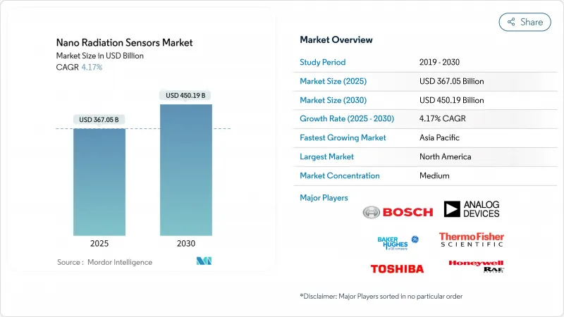
The nano radiation sensors market stood at USD 367.05 billion in 2025 and is forecast to register a 4.17% CAGR, reaching USD 450.19 billion by 2030.
Growth reflects consistent miniaturization across consumer electronics, aerospace, and automotive systems, paired with stringent safety rules in nuclear decommissioning and space exploration. Recent breakthroughs in perovskite semiconductor materials now allow detector footprints small enough for smartphone integration and wearable patches, removing long-standing size and power barriers. Government stimulus ranging from the GBP 30 million package under the UK Nuclear Decommissioning Authority to the USD 105 million CHIPS Act grant for Analog Devices shortens commercialization cycles and accelerates supply expansion. CubeSat proliferation, particularly in university and startup missions, compounds the addressable volume for ultra-light sensors, while parallel demand arises from healthcare dosimetry and automotive safety subsystems. Manufacturing complexity and yield losses remain the most significant constraints; however, firms that resolve material-stability issues while maintaining cost control gain an immediate competitive edge.
Global Nano Radiation Sensors Market Trends and Insights
Miniaturization trend across industries
Relentless downsizing in consumer electronics and automotive platforms pushes radiation sensor modules toward wafer-level integration. Sharp demonstrated a 25 X 20 X 2.5 mm module drawing only 7.5 mW, making smartphone-based radiation tracking practical. Parallel progress in 5 nm and 3 nm process nodes allows logic and detection circuitry to share a common die, lowering bill-of-materials costs for original-equipment manufacturers. In automobiles, compact sensors now fit inside existing electronic control units, supporting Advanced Driver Assistance Systems without altering cabin design. As IoT architectures spread, distributed nano radiation sensors can be deployed in factories and hospitals at node-level costs that were unattainable five years ago.
Government nanotech funding and standards
Targeted public programs guarantee long-term demand while harmonizing certification. The U.S. Department of Commerce earmarked USD 105 million for Analog Devices to modernize three domestic fabs, explicitly citing commercial and defense radiation detection as priority outputs. The UK Nuclear Decommissioning Authority injected GBP 30 million into sensor R & D to support safe dismantling of legacy reactors. In parallel, the European Commission's Horizon Europe platform directs resources toward sustainable radiation-protection technology. ISO and IEEE working groups now draft unified nano sensor test protocols that cut compliance cycles and enable cross-border procurement.
Manufacturing complexity and yield losses
Sub-10 nm features needed for latest detector architectures experience higher defect rates than mainstream logic chips, depressing first-pass yields below 60% at several foundries. Supply-chain shocks-such as the temporary shutdown of Spruce Pine's quartz mine that feeds high-purity silica into photolithography mask blanks-amplify cost pressures by constricting vital materials. Fab operators must adopt tighter particulate controls and advanced metrology, driving up per-wafer operating expenses in the short run.
Other drivers and restraints analyzed in the detailed report include:
- Growing demand for high-precision healthcare dosimetry
- Nuclear decommissioning and safety regulations
- Stability issues of perovskite / organic materials
For complete list of drivers and restraints, kindly check the Table Of Contents.
Segment Analysis
Solid-state detectors captured 58% of 2024 revenue within the nano radiation sensors market, leveraging CMOS compatibility to embed sensing elements directly onto mixed-signal chips. This architecture trims power budgets and simplifies board layouts, attributes valued in medical imaging consoles and satellite payloads. Scintillation units, though smaller in share, benefit from 6.5% CAGR prospects tied to perovskite nanocrystal breakthroughs delivering light yields above 100,000 photons MeV-1. Hybrid designs now merge solid-state readout with nanocrystal scintillators, achieving sub-400 ps response while retaining wafer-level processing economies.
Second-generation solid-state platforms adopt nano-plasmonic enhancement layers that triple photon-collection efficiency without expanding footprint. As perovskite coatings mature, manufacturers experiment with monolithic integration of high-Z scintillators atop silicon photodiodes, pointing toward single-chip gamma cameras for endoscopic surgery. The evolution indicates that categorical boundaries between solid-state and scintillation approaches will blur, generating new revenue pools throughout the nano radiation sensors industry.
Silicon maintained 46% contribution to 2024 revenue, offering reliable supply and extensive foundry support that underpins the current nano radiation sensors market size for mainstream applications. Production learning curves keep average selling prices predictable, a trait essential for automotive Tier-1 suppliers committing to decade-long product cycles. Perovskite detectors, at 8.2% CAGR, benefit from solution processing that allows roll-to-roll coating of flexible substrates, widening addressable opportunities in wearable health monitors and drone platforms.
Composite stacks merging silicon ASICs with thin perovskite absorber layers allow detection of soft X-ray and low-energy gamma photons in a single envelope, improving multispectral imaging for nondestructive testing. Lead-free compositions featuring manganese complexes reach photoluminescence quantum yields above 80%, providing an environmental upgrade without sacrificing detection efficiency. These hybrid stacks signal an inflection point where material-choice decisions become application-specific rather than supply-chain constrained.
Nano Radiation Sensors Market Segmented by Type (Scintillation Detectors, Solid-State Detectors), Material (Silicon-Based Semiconductors, Inorganic Crystals (GAGG, LSO, Csi) and More), Application (Automotive, Consumer Electronics and More), Technology, Indirect Scintillation-CMOS and More), Detection Radiation Type, Form Factor and Geography. The Market Forecasts are Provided in Terms of Value (USD).
Geography Analysis
North American leadership, with 35% 2024 share, is anchored by continuous defense procurement and multi-billion-dollar modernization across 93 operating nuclear reactors. Analog Devices is tripling wafer starts in Massachusetts and Oregon under the CHIPS Act, securing long-run availability of military-grade detectors. Thermo Fisher's enlarged US network of 64 manufacturing sites reinforces domestic supply for healthcare, industrial NDT, and homeland-security programs, while AI-augmented monitoring at two US pressurized-water reactors cuts unscheduled outage hours through predictive analytics.
APAC shows the fastest 5.9% CAGR forecast, underpinned by China's successful scaling of smartphone-compatible radiation chips, which broaden public-safety adoption. Japan maintains domain expertise via Sharp's ultra-thin sensor module and JAEA's silicon gamma-ray detectors qualified for boiling-water reactor retrofits. South Korea's LEO-DOS payload on NEXTSat-2 validates homegrown radiation-hard designs for low-Earth-orbit dosimetry, signalling export-ready competence for emerging space economies in Southeast Asia.
Europe prioritizes safe dismantling of 171 GW of nuclear capacity set for phase-out before 2050, creating near-term demand peaks for distributed sensor arrays. The UK's GBP 30 million research grant seeds university-industry consortia to prototype autonomous robotic monitors. Germany's automotive Tier-1 suppliers explore integrating radiation sensing into ADAS control units to certify electronics against single-event upsets, while France's EDF upgrades core flux mapping with nano sensors to extend plant licenses beyond 60 years. Finland's University of Jyvaskyla produced a handheld multi-purpose detector that merges neutron, gamma, and beta channels, supporting first-responder toolkits across the continent.
- Analog Devices Inc.
- Robert Bosch GmbH
- Nihon Kessho Kogaku Co. Ltd.
- Thermo Fisher Scientific Inc.
- Baker Hughes Co.
- Honeywell International Inc. (RAE Systems)
- First Sensor AG (TE Connectivity)
- Hamamatsu Photonics KK
- Toshiba Corporation
- Mirion Technologies Inc.
- Fortive Corporation
- PerkinElmer Inc. (Revvity)
- Radiation Monitoring Devices Inc.
- Texas Instruments Inc.
- Lockheed Martin Corp.
- OMRON Corporation
- Space Micro Inc.
- Analogic Corporation
- Canon Medical Systems Corp.
- Siemens Healthineers AG
- GE Healthcare Technologies Inc.
- BAE Systems plc
- Hitachi Ltd.
- STMicroelectronics N.V.
Additional Benefits:
- The market estimate (ME) sheet in Excel format
- 3 months of analyst support
TABLE OF CONTENTS
1 INTRODUCTION
- 1.1 Study Assumptions and Market Definition
- 1.2 Scope of the Study
2 RESEARCH METHODOLOGY
3 EXECUTIVE SUMMARY
4 MARKET LANDSCAPE
- 4.1 Market Overview
- 4.2 Market Drivers
- 4.2.1 Miniaturization trend across industries
- 4.2.2 Government nanotech funding and standards
- 4.2.3 Growing demand for high-precision healthcare dosimetry
- 4.2.4 Nuclear decommissioning and safety regulations
- 4.2.5 CubeSat and small-sat adoption of nano-sensors
- 4.2.6 Flexible perovskite scintillators enable wearable dosimetry
- 4.3 Market Restraints
- 4.3.1 Manufacturing complexity and yield losses
- 4.3.2 High capital cost of nano-fabrication lines
- 4.3.3 Lack of integration standards across OEMs
- 4.3.4 Stability issues of perovskite / organic materials
- 4.4 Value / Supply-Chain Analysis
- 4.5 Regulatory Landscape
- 4.6 Technological Outlook
- 4.7 Key Performance Indicators (KPIs)
- 4.8 Porter's Five Forces Analysis
- 4.8.1 Threat of New Entrants
- 4.8.2 Bargaining Power of Buyers
- 4.8.3 Bargaining Power of Suppliers
- 4.8.4 Threat of Substitutes
- 4.8.5 Intensity of Competitive Rivalry
5 MARKET SIZE AND GROWTH FORECASTS (VALUE)
- 5.1 By Type
- 5.1.1 Scintillation Detectors
- 5.1.2 Solid-state Detectors
- 5.2 By Material
- 5.2.1 Silicon-based Semiconductors
- 5.2.2 Inorganic Crystals (GAGG, LSO, CsI)
- 5.2.3 Perovskite Semiconductors (Lead and Lead-free)
- 5.2.4 Organic / Polymer Scintillators
- 5.3 By Application
- 5.3.1 Automotive
- 5.3.2 Consumer Electronics
- 5.3.3 Healthcare
- 5.3.4 Industrial
- 5.3.5 Oil and Gas
- 5.3.6 Power Generation
- 5.3.7 Other Applications
- 5.4 By Technology
- 5.4.1 Direct-conversion (Photon-counting)
- 5.4.2 Indirect Scintillation-CMOS
- 5.4.3 Flexible / Wearable Panels
- 5.4.4 Radiation-hardened SoC and SiPM
- 5.5 By Detection Radiation Type
- 5.5.1 Alpha
- 5.5.2 Beta
- 5.5.3 Gamma / X-ray
- 5.5.4 Neutron
- 5.6 By Form Factor
- 5.6.1 Chip-scale
- 5.6.2 Module
- 5.6.3 Panel
- 5.6.4 Wearable Patch
- 5.7 By Geography
- 5.7.1 North America
- 5.7.1.1 United States
- 5.7.1.2 Canada
- 5.7.1.3 Mexico
- 5.7.2 South America
- 5.7.2.1 Brazil
- 5.7.2.2 Argentina
- 5.7.2.3 Rest of South America
- 5.7.3 Europe
- 5.7.3.1 United Kingdom
- 5.7.3.2 Germany
- 5.7.3.3 France
- 5.7.3.4 Italy
- 5.7.3.5 Russia
- 5.7.3.6 Spain
- 5.7.3.7 Rest of Europe
- 5.7.4 Asia-Pacific
- 5.7.4.1 China
- 5.7.4.2 Japan
- 5.7.4.3 India
- 5.7.4.4 South Korea
- 5.7.4.5 Rest of Asia-Pacific
- 5.7.5 Middle East and Africa
- 5.7.5.1 Middle East
- 5.7.5.1.1 United Arab Emirates
- 5.7.5.1.2 Saudi Arabia
- 5.7.5.1.3 Turkey
- 5.7.5.1.4 Rest of Middle East
- 5.7.5.2 Africa
- 5.7.5.2.1 South Africa
- 5.7.5.2.2 Egypt
- 5.7.5.2.3 Rest of Africa
- 5.7.1 North America
6 COMPETITIVE LANDSCAPE
- 6.1 Market Concentration
- 6.2 Strategic Moves
- 6.3 Market Share Analysis
- 6.4 Company Profiles {(includes Global level Overview, Market level overview, Core Segments, Financials as available, Strategic Information, Market Rank/Share for key companies, Products and Services, and Recent Developments)}
- 6.4.1 Analog Devices Inc.
- 6.4.2 Robert Bosch GmbH
- 6.4.3 Nihon Kessho Kogaku Co. Ltd.
- 6.4.4 Thermo Fisher Scientific Inc.
- 6.4.5 Baker Hughes Co.
- 6.4.6 Honeywell International Inc. (RAE Systems)
- 6.4.7 First Sensor AG (TE Connectivity)
- 6.4.8 Hamamatsu Photonics KK
- 6.4.9 Toshiba Corporation
- 6.4.10 Mirion Technologies Inc.
- 6.4.11 Fortive Corporation
- 6.4.12 PerkinElmer Inc. (Revvity)
- 6.4.13 Radiation Monitoring Devices Inc.
- 6.4.14 Texas Instruments Inc.
- 6.4.15 Lockheed Martin Corp.
- 6.4.16 OMRON Corporation
- 6.4.17 Space Micro Inc.
- 6.4.18 Analogic Corporation
- 6.4.19 Canon Medical Systems Corp.
- 6.4.20 Siemens Healthineers AG
- 6.4.21 GE Healthcare Technologies Inc.
- 6.4.22 BAE Systems plc
- 6.4.23 Hitachi Ltd.
- 6.4.24 STMicroelectronics N.V.
7 MARKET OPPORTUNITIES AND FUTURE OUTLOOK
- 7.1 White-space and Unmet-need Assessment

