
PUBLISHER: Mordor Intelligence | PRODUCT CODE: 1849924

PUBLISHER: Mordor Intelligence | PRODUCT CODE: 1849924
Semiconductor Packaging - Market Share Analysis, Industry Trends & Statistics, Growth Forecasts (2025 - 2030)
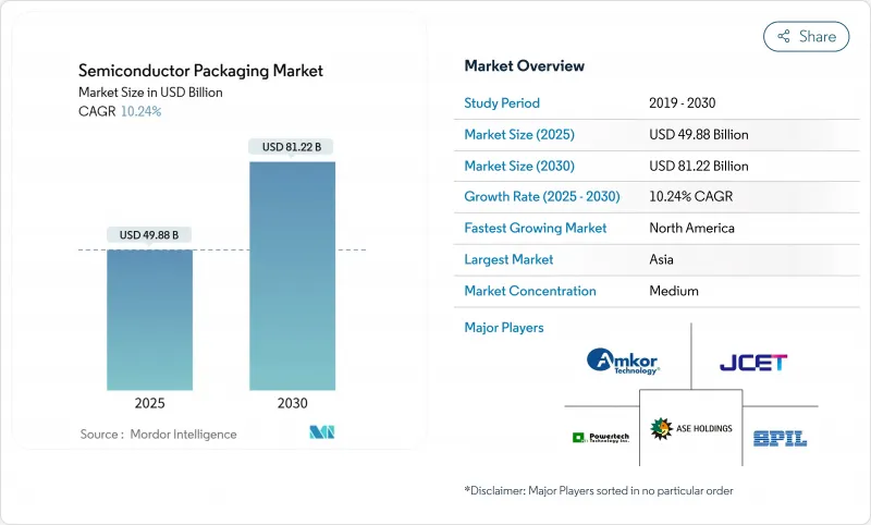
The semiconductor packaging market size stood at USD 49.88 billion in 2025 and is projected to reach USD 81.22 billion by 2030, advancing at a 10.24% CAGR over 2025-2030.
A shift from cost-driven assembly toward performance-critical integration underpins this growth. Demand for 2.5D and 3D architectures has risen sharply as AI workloads call for high-bandwidth memory and superior thermal paths. Volume remains anchored in traditional wire-bond and lead-frame formats, yet value creation is migrating to fan-out wafer-level packaging (WLP) and chiplet-enabled interposers. Automotive electrification supports double-digit expansion in power-dense modules, while smartphone and PC refresh cycles sustain baseline volumes in the consumer segment. Regionally, Asia commands more than half of global output, but North America registers the highest CAGR thanks to CHIPS Act incentives that fund new back-end fabs. Supply bottlenecks in ABF substrates and export restrictions on advanced tools are catalyzing geographic diversification and material innovation.
Global Semiconductor Packaging Market Trends and Insights
AI accelerator boom driving 2.5D/3D interposers
TSMC's CoWoS capacity is doubling from 120,000 to 240,000 units between 2023 and 2024, yet it still cannot fully meet hyperscaler demand. The capacity gap is stimulating alternative panel-level flows and 3.5D stacking trials that aggregate more than 6,000 mm2 of silicon per package. Advanced packaging has therefore moved from a cost center to a strategic lever for AI system performance
Electrified-vehicle power packages in United States & Asia
onsemi's EliteSiC platform awarded by Volkswagen exemplifies the migration toward integrated power modules with superior heat dissipation. ROHM's 6-in-1 molded SiC modules deliver triple the power density of prior. These innovations concentrate in US and Asian supply chains that can meet stringent automotive qualification.
ABF substrate supply crunch
Nittobo's 20% price hike in August 2025 exposes systemic material tightness that particularly affects flip-chip BGA lines. Limited qualified capacity in Taiwan and Japan prolongs lead times and pushes OEMs to explore glass-core or silicon-core alternatives.
Other drivers and restraints analyzed in the detailed report include:
- US-EU CHIPS incentives creating local back-end fabs
- 5G RF-SiP demand in China & Korea
- Yield challenges in 3D TSV/hybrid bonding
For complete list of drivers and restraints, kindly check the Table Of Contents.
Segment Analysis
Traditional wire-bond and lead-frame offerings still dominated shipments with 52.5% semiconductor packaging market share in 2024, ensuring that consumer electronics and industrial devices retain affordable bill-of-materials costs. However, Fan-out WLP outpaces every other format at a 12.3% CAGR, signaling the semiconductor packaging market's move toward substrate-free redistribution layers that shrink z-height and boost I/O density. Flip-chip bridges the gap by pairing fine-pitch bumps with moderate cost, while SiP and PoP architectures enable vertical stacking for space-constrained handsets.
On the advanced front, 2.5D interposers position high-bandwidth memory adjacent to AI logic, and 3D stacks unlock latency gains. Embedded-die and panel-level flows attract new entrants focused on IoT price points, demonstrating that the semiconductor packaging market is splitting into premium performance nodes and ultra-low-cost volume plays. In contrast, panel-level lines deliver sub-USD 0.10 per pin, a ratio that underscores divergent cost structures. As a result, equipment makers have segmented their portfolios: high-accuracy bonder clusters for 3 µm alignment coexist with large-panel MOLD lines aimed at IoT tags. Such bifurcation redefines supplier positioning inside the semiconductor packaging market.
Organic ABF substrates carried 41.5% revenue in 2024, underpinning the mainstream flip-chip ecosystem. Yet semiconductor packaging market size for bonding wires is set to grow 11.4% annually as automotive and industrial sectors extend the life of proven aluminum and gold wire packages. Leadframes persist in power applications that value copper heat-spreader performance. Encapsulation resins have progressed to high-thermal-conductivity grades, supporting next-generation SiC and GaN modules.
Glass substrates could displace organic builds after 2027. Intel and Samsung prototypes show 40% via pitch reduction and near-zero CTE mismatch, lowering warpage in 3D stacks. Thermal interface materials now integrate nano-diamond fillers, cutting junction-to-case resistance by 30% in 1,200 V traction inverters. Gold price spikes compressed margins for display driver IC packaging in 2025, motivating migration to copper column bumps
The Semiconductor Packaging Market is Segmented by Packaging Platform (Advanced Packaging, Traditional Packaging), Packaging Material (Organic Substrates, and More), Wafer Size (<= 200 Mm, and More), Business Model (OSAT, and More) End-User Industry (Consumer Electronics, Aerospace and Defense and More), and by Geography. The Market Forecasts are Provided in Terms of Value (USD).
Geography Analysis
Asia captured 53.0% of the semiconductor packaging market in 2024, cemented by Taiwan's CoWoS monopoly and China's scale in wire-bond assembly. JCET's RMB 4.4 billion automotive plant in Jiangsu advances local competency in SiC power packages. South Korea benefits from memory-centric SiP, whereas Japan controls pivotal substrate chemistries, reinforcing a tightly knit regional cluster.
North America's semiconductor packaging market is projected to post an 11.1% CAGR through 2030. CHIPS Act incentives amass USD 300 million for R&D lines, spawning hubs in Arizona, New Mexico and California. Partnerships such as TSMC-Amkor in Arizona build complete back-end ecosystems proximate to leading-edge wafer fabs. Canada cultivates photonics packaging, and Mexico offers low-cost final test for consumer ASICs.
Europe positions around automotive and industrial strength. German Tier-1s co-develop double-sided cooled SiC modules targeting 9 kW/L inverter density, catalyzing niche OSAT investment. The Netherlands pushes high-frequency optical transceiver packaging that aligns with vertical-cavity surface-emitting laser (VCSEL) adoption. Middle East and Africa remain emerging, primarily outsourcing assembly to Asian hubs yet planning domestic lines for secure IoT and defense electronics under sovereign mandates.
- ASE Technology Holding Co., Ltd.
- Amkor Technology, Inc.
- JCET Group Co., Ltd.
- Siliconware Precision Industries Co., Ltd.
- Powertech Technology Inc.
- Tianshui Huatian Technology Co., Ltd.
- UTAC Holdings Ltd.
- ChipMOS Technologies Inc.
- Chipbond Technology Corp.
- Intel Corporation
- Samsung Electronics Co., Ltd.
- Taiwan Semiconductor Manufacturing Co. Ltd. (TSMC)
- Micron Technology, Inc.
- Texas Instruments Inc.
- Advanced Micro Devices, Inc.
- Hana Micron Inc.
- Nepes Corporation
- TongFu Microelectronics Co., Ltd.
- Shinko Electric Industries Co., Ltd.
- Unisem (M) Berhad
Additional Benefits:
- The market estimate (ME) sheet in Excel format
- 3 months of analyst support
TABLE OF CONTENTS
1 INTRODUCTION
- 1.1 Study Assumptions and Market Definition
- 1.2 Scope of the Study
2 RESEARCH METHODOLOGY
3 EXECUTIVE SUMMARY
4 MARKET LANDSCAPE
- 4.1 Market Overview
- 4.2 Market Drivers
- 4.2.1 AI Accelerator Boom Driving 2.5D/3D Interposers
- 4.2.2 Electrified Vehicle Power Packages in United States and Asia
- 4.2.3 US-EU CHIPS Incentives Creating Local Back-End Fabs
- 4.2.4 5G RF-SiP Demand in China and Korea
- 4.2.5 Panel Level Packaging for Ultra-Low-Cost IoT
- 4.2.6 Chiplet Architectures Powering High-Density Interposers
- 4.3 Market Restraints
- 4.3.1 ABF Substrate Supply Crunch (Taiwan/Japan)
- 4.3.2 Yield Challenges in 3D TSV/Hybrid Bonding
- 4.3.3 Export Controls on Advanced Packaging Tools to China
- 4.3.4 Thermal Dissipation Limits in Fan-Out WLP @ <5 nm
- 4.4 Value / Supply-Chain Analysis
- 4.5 Regulatory Outlook
- 4.6 Technological Outlook
- 4.7 Porter's Five Forces
- 4.7.1 Bargaining Power of Suppliers
- 4.7.2 Bargaining Power of Buyers
- 4.7.3 Threat of New Entrants
- 4.7.4 Threat of Substitutes
- 4.7.5 Intensity of Competitive Rivalry
- 4.8 Industry Capacity and Investment Trend Analysis
- 4.9 Pricing Analysis
5 MARKET SIZE AND GROWTH FORECASTS (VALUE)
- 5.1 By Packaging Platform
- 5.1.1 Advanced Packaging
- 5.1.1.1 Flip-Chip
- 5.1.1.2 Fan-Out WLP
- 5.1.1.3 Fan-In WLP
- 5.1.1.4 2.5D / 3D IC
- 5.1.1.5 Embedded-Die
- 5.1.1.6 SiP / PoP
- 5.1.1.7 Panel-Level Packaging
- 5.1.2 Traditional Packaging
- 5.1.2.1 Wire-Bond
- 5.1.2.2 Leadframe
- 5.1.2.3 QFN / QFP / SOP
- 5.1.1 Advanced Packaging
- 5.2 By Packaging Material
- 5.2.1 Organic Substrates
- 5.2.2 Leadframes
- 5.2.3 Bonding Wires
- 5.2.4 Encapsulation Resins
- 5.2.5 Ceramic Packages
- 5.2.6 Solder Balls and Bumps
- 5.2.7 Die-Attach and TIMs
- 5.3 By Wafer Size
- 5.3.1 <= 200 mm
- 5.3.2 300 mm
- 5.3.3 >= 450 mm / Panel
- 5.4 By Business Model
- 5.4.1 OSAT
- 5.4.2 Foundry Back-End
- 5.4.3 IDM In-house
- 5.5 By End-user Industry
- 5.5.1 Consumer Electronics
- 5.5.1.1 Smartphones and Wearables
- 5.5.1.2 Computing / Data-Center
- 5.5.1.3 Automotive and Mobility
- 5.5.1.3.1 ADAS / EV Power
- 5.5.1.4 Communications and Telecom
- 5.5.1.4.1 5G Infrastructure
- 5.5.1.5 Aerospace and Defense
- 5.5.1.6 Medical and Healthcare Devices
- 5.5.1.7 Industrial and Energy (LED / Power)
- 5.5.1 Consumer Electronics
- 5.6 By Geography
- 5.6.1 North America
- 5.6.1.1 United States
- 5.6.1.2 Canada
- 5.6.1.3 Mexico
- 5.6.2 South America
- 5.6.2.1 Brazil
- 5.6.2.2 Rest of South America
- 5.6.3 Europe
- 5.6.3.1 Germany
- 5.6.3.2 France
- 5.6.3.3 United Kingdom
- 5.6.3.4 Italy
- 5.6.3.5 Netherlands
- 5.6.3.6 Nordics
- 5.6.3.7 Rest of Europe
- 5.6.4 Middle East and Africa
- 5.6.4.1 Israel
- 5.6.4.2 Turkey
- 5.6.4.3 GCC
- 5.6.4.4 South Africa
- 5.6.4.5 Rest of Middle East and Africa
- 5.6.5 APAC
- 5.6.5.1 China
- 5.6.5.2 Taiwan
- 5.6.5.3 South Korea
- 5.6.5.4 Japan
- 5.6.5.5 India
- 5.6.5.6 Singapore
- 5.6.5.7 Australia
- 5.6.5.8 New Zealand
- 5.6.5.9 Rest of APAC
- 5.6.1 North America
6 Competitive Landscape
- 6.1 Market Concentration
- 6.2 Strategic Moves
- 6.3 Market Share Analysis
- 6.4 Company Profiles (includes Global level Overview, Market level overview, Core Segments, Financials as available, Strategic Information, Market Rank/Share, Products & Services, Recent Developments)
- 6.4.1 ASE Technology Holding Co., Ltd.
- 6.4.2 Amkor Technology, Inc.
- 6.4.3 JCET Group Co., Ltd.
- 6.4.4 Siliconware Precision Industries Co., Ltd.
- 6.4.5 Powertech Technology Inc.
- 6.4.6 Tianshui Huatian Technology Co., Ltd.
- 6.4.7 UTAC Holdings Ltd.
- 6.4.8 ChipMOS Technologies Inc.
- 6.4.9 Chipbond Technology Corp.
- 6.4.10 Intel Corporation
- 6.4.11 Samsung Electronics Co., Ltd.
- 6.4.12 Taiwan Semiconductor Manufacturing Co. Ltd. (TSMC)
- 6.4.13 Micron Technology, Inc.
- 6.4.14 Texas Instruments Inc.
- 6.4.15 Advanced Micro Devices, Inc.
- 6.4.16 Hana Micron Inc.
- 6.4.17 Nepes Corporation
- 6.4.18 TongFu Microelectronics Co., Ltd.
- 6.4.19 Shinko Electric Industries Co., Ltd.
- 6.4.20 Unisem (M) Berhad
7 MARKET OPPORTUNITIES AND FUTURE OUTLOOK
- 7.1 White-space and Unmet-Need Assessment

