
PUBLISHER: Mordor Intelligence | PRODUCT CODE: 1850971

PUBLISHER: Mordor Intelligence | PRODUCT CODE: 1850971
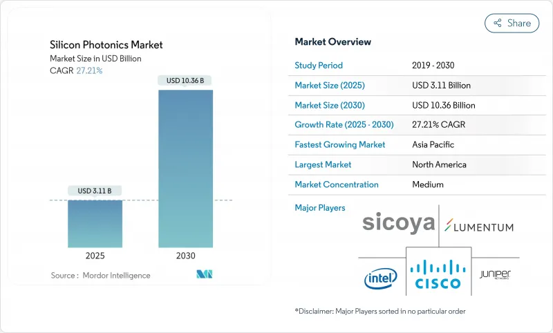
Silicon Photonics - Market Share Analysis, Industry Trends & Statistics, Growth Forecasts (2025 - 2030)
The silicon photonics market generates USD 3.11 billion in 2025 and is forecast to advance at a 27.21% CAGR, reaching USD 10.36 billion by 2030.
Demand is accelerating as hyperscale data centers shift from 800 G to 1.6 T optical links, automotive OEMs integrate frequency-modulated continuous-wave LiDAR, and government incentives expand domestic semiconductor capacity. North America retains leadership, yet Asia Pacific is closing the gap through large-scale fab expansions aligned with 5G, AI and sovereign-supply objectives. Competing material platforms such as indium phosphide spur innovation but also intensify price pressure, while thermal-budget ceilings above 70 °C force new cooling architectures. M&A activity underscores the rising strategic value of photonic integration, with network equipment vendors, foundries and cloud providers securing design teams and wafer capacity ahead of looming supply constraints.
Global Silicon Photonics Market Trends and Insights
Energy-efficient Co-Packaged Optics Adoption in Hyperscale Data Centers
Directly embedding optical engines beside switch ASICs trims electrical-optical conversions and cuts rack-level power draw by up to 40%. Google's optical circuit switching trials validate latency gains, and both NVIDIA and Marvell now sample proprietary co-packaged modules that streamline board layouts for AI clusters. The silicon photonics market benefits as switch makers standardize optical die-to-die interfaces, creating a volume pull for integrated lasers, modulators and photodetectors packaged on 300 mm wafers.
Carbon-Reduction Mandates Driving Low-Power Optical Interconnects
EU data-center sustainability rules target significant energy savings, prompting operators to phase out copper backplanes. Photonic links show 30% lower consumption in 100 Gbps channels while maintaining reach. Cloud providers publish carbon-neutral roadmaps, accelerating multi-vendor qualification of 400 G and 800 G silicon photonics modules that align with corporate ESG metrics and local green-deal incentives.
Thermal Budget Limitations in Silicon Substrates Above 70 °C
Optical phase stability drops at elevated junction temperatures, forcing elaborate heat sinks and liquid cooling in tightly packed AI servers.Research programs explore heterogeneous materials with higher thermal conductivity and temperature-insensitive resonator designs, yet these add process steps and cost, tempering near-term adoption in edge compute nodes.
Other drivers and restraints analyzed in the detailed report include:
- 5G Fronthaul/Backhaul Upgrade Fueling 400/800 G Modules
- Automotive Level-3 LiDAR Programs Leveraging FMCW Silicon Photonics
- Lack of Standardized Packaging Elevating NRE Costs
For complete list of drivers and restraints, kindly check the Table Of Contents.
Segment Analysis
Optical transceivers generated 62% revenue in 2024 as hyperscalers deployed 800 G optics and qualified early 1.6 T line-cards.Design wins increasingly bundle integrated drivers and thermal monitors, easing system design and lowering capex per port. The silicon photonics market continues to pivot toward full-stack transceiver solutions that collapse laser, modulator and photodetector in one monolithic die. Market entrants differentiate through modal multiplexing and CW-laser integration that improve power efficiency.
Wafer-level test systems show the fastest expansion at 28.1% CAGR, propelled by tighter yield requirements at 400-G symbols /s and above. Parallel optical probing shrinks cycle time and raises throughput to match 300 mm line capacity. Vendors invest in AI-assisted defect analytics, linking parametric drift to fab data and enabling predictive maintenance. Broader use of automated optical test shortens time-to-qualification for new tape-outs, buttressing scale-up of the silicon photonics market.
Active components maintained a 58% share in 2024, reflecting persistent demand for compact CW lasers, high-extinction modulators and low-dark-current photodiodes. Integrated multiplexers now ship in 112Gbaud PAM4 transceivers, demonstrating stable drive voltages at 55 °C case temperatures. Chip makers refine heterogeneous III-V laser attach, boosting wall-plug efficiency and reducing optical loss across epitaxial interfaces.
Passive components post the highest 29.7% CAGR as fabs iterate low-loss waveguides, lattice filters and arrayed-waveguide gratings tailored for 400G ZR+. Ultralow-roughness etch profiles cut insertion loss below 0.5 dB/cm, essential for co-packaged optics. Printed photonic circuit boards embedding glass waveguides promise board-level optical backplanes, further expanding addressable opportunities for the silicon photonics market.
The Silicon Photonics Market Report is Segmented by Product (Optical Transceivers, Optical Switches, and More), Component (Active, and Passive), Wafer Size (300 Mm, 200 Mm, 150 Mm and Below), Application (Data Centers and High-Performance Computing, Telecommunications, and More), End-User (Hyperscale Cloud Providers, Telecom Operators, and More), and Geography. The Market Forecasts are Provided in Terms of Value (USD).
Geography Analysis
North America generated 38% of 2024 revenue, buoyed by CHIPS Act grants and rapid deployment of AI mega-campuses. Albany NanoTech's elevation to national research hub and private-sector investments from cloud leaders lock in a domestic ecosystem spanning design, packaging and advanced testing. Ongoing evolution of the silicon photonics market in the region hinges on seamless collaboration between foundries and equipment vendors to overcome wafer-level thermal setbacks.
Asia Pacific records the fastest 35.1% CAGR through 2030 as China, Japan and South Korea race to anchor sovereign supply chains. Government subsidies cover fab tools, training and metrology, while 5G densification and local AI start-ups guarantee offtake. Japanese investments in 300 mm GaAs-on-silicon lasers position domestic suppliers for export-oriented growth, reinforcing the global breadth of the silicon photonics market.
Europe sustains momentum through the EU Chips Act's multi-billion-euro financing and a strong industrial base in automotive, industrial automation and research photonics. Carbon-neutral data-center mandates further encourage photonic adoption. South America and the Middle East & Africa open new footholds for telecom and edge-cloud deployments, but still rely on imported dies and packaging services, a gap that multinational OEMs strive to close via localized assembly partnerships.
- Intel Corporation
- Cisco Systems Inc.
- Broadcom Inc.
- Lumentum Holdings Inc.
- Juniper Networks Inc.
- GlobalFoundries Inc.
- Sicoya GmbH
- Molex LLC
- Marvell Technology Inc.
- MACOM Technology Solutions
- Coherent Corp.
- Hamamatsu Photonics K.K.
- Ayar Labs Inc.
- NeoPhotonics Corp.
- IBM Corporation
- Hewlett Packard Enterprise
- II-VI Inc. (now Coherent)
- Rockley Photonics
- Infinera Corporation
- Smart Photonics
- DustPhotonics
- PsiQuantum
- POET Technologies
- Tower Semiconductor
Additional Benefits:
- The market estimate (ME) sheet in Excel format
- 3 months of analyst support
TABLE OF CONTENTS
1 INTRODUCTION
- 1.1 Study Assumptions and Market Definition
- 1.2 Scope of the Study
2 RESEARCH METHODOLOGY
3 EXECUTIVE SUMMARY
4 MARKET LANDSCAPE
- 4.1 Market Overview
- 4.2 Market Drivers
- 4.2.1 Energy-Efficient Co-Packaged Optics Adoption in Hyperscale Data Centers (North America)
- 4.2.2 Carbon-Reduction Mandates Driving Low-Power Optical Interconnects (EU)
- 4.2.3 5G Fronthaul/Backhaul Upgrade Fueling 400/800 G Modules (Asia)
- 4.2.4 Automotive Level-3 LiDAR Programs Leveraging FMCW Silicon Photonics (China and EU)
- 4.2.5 Defense Funding for Quantum and Secure Photonics (United States)
- 4.2.6 Government Semiconductor Incentive Schemes Expanding Photonic Fabs (US/EU/Asia)
- 4.3 Market Restraints
- 4.3.1 Thermal Budget Limitations in Silicon Substrates Above 70 °C
- 4.3.2 Lack of Standardized Packaging Elevating NRE Costs
- 4.3.3 Competition from InP and Polymer Photonics Beyond 1.55 µm
- 4.3.4 Limited 300 mm Photonic Foundry capacity Causing Extended Lead Times
- 4.4 Industry Ecosystem Analysis
- 4.5 Regulatory Outlook
- 4.6 Technological Outlook
- 4.7 Porter's Five Forces Analysis
- 4.7.1 Bargaining Power of Suppliers
- 4.7.2 Bargaining Power of Buyers
- 4.7.3 Threat of New Entrants
- 4.7.4 Threat of Substitutes
- 4.7.5 Intensity of Competitive Rivalry
5 MARKET SIZE AND GROWTH FORECASTS (VALUES)
- 5.1 By Product
- 5.1.1 Optical Transceivers
- 5.1.2 Optical Switches
- 5.1.3 Active Optical Cables (AOCs)
- 5.1.4 Silicon Photonic Sensors
- 5.1.5 Wafer-level Test Systems
- 5.1.6 Multiplexers/De-Multiplexers
- 5.1.7 Attenuators and Modulators
- 5.1.8 Others
- 5.2 By Component
- 5.2.1 Active Components
- 5.2.1.1 Lasers
- 5.2.1.2 Modulators
- 5.2.1.3 Photodetectors
- 5.2.2 Passive Components
- 5.2.2.1 Waveguides
- 5.2.2.2 Filters
- 5.2.2.3 Couplers
- 5.2.2.4 Others
- 5.2.1 Active Components
- 5.3 By Wafer Size
- 5.3.1 300 mm
- 5.3.2 200 mm
- 5.3.3 150 mm and Below
- 5.4 By Data Rate
- 5.4.1 ?100 Gbps
- 5.4.2 200 Gbps
- 5.4.3 400 Gbps
- 5.4.4 800 Gbps
- 5.4.5 ?1.6 Tbps
- 5.5 By Application
- 5.5.1 Data Centers and High-Performance Computing
- 5.5.2 Telecommunications
- 5.5.3 Automotive and Autonomous Vehicles
- 5.5.4 AR/VR and Consumer Electronics
- 5.5.5 Healthcare and Life Sciences
- 5.5.6 Defense and Aerospace
- 5.5.7 Quantum Computing
- 5.5.8 Others
- 5.6 By End-User
- 5.6.1 Hyperscale Cloud Providers
- 5.6.2 Telecom Operators
- 5.6.3 Automotive OEMs and Tier-1 Suppliers
- 5.6.4 Medical Device Manufacturers
- 5.6.5 Government and Defense Agencies
- 5.6.6 Research and Academic Institutions
- 5.7 By Geography
- 5.7.1 North America
- 5.7.1.1 United States
- 5.7.1.2 Canada
- 5.7.1.3 Mexico
- 5.7.2 Europe
- 5.7.2.1 Germany
- 5.7.2.2 United Kingdom
- 5.7.2.3 France
- 5.7.2.4 Italy
- 5.7.2.5 Spain
- 5.7.2.6 Rest of Europe
- 5.7.3 Asia-Pacific
- 5.7.3.1 China
- 5.7.3.2 Japan
- 5.7.3.3 South Korea
- 5.7.3.4 India
- 5.7.3.5 South East Asia
- 5.7.3.6 Australia
- 5.7.3.7 Rest of Asia-Pacific
- 5.7.4 South America
- 5.7.4.1 Brazil
- 5.7.4.2 Rest of South America
- 5.7.5 Middle East and Africa
- 5.7.5.1 Middle East
- 5.7.5.1.1 United Arab Emirates
- 5.7.5.1.2 Saudi Arabia
- 5.7.5.1.3 Rest of Middle East
- 5.7.5.2 Africa
- 5.7.5.2.1 South Africa
- 5.7.5.2.2 Rest of Africa
- 5.7.1 North America
6 COMPETITIVE LANDSCAPE
- 6.1 Market Concentration
- 6.2 Strategic Moves
- 6.3 Market Share Analysis
- 6.4 Company Profiles (includes Global level Overview, Market level overview, Core Segments, Financials as available, Strategic Information, Market Rank/Share for key companies, Products and Services, and Recent Developments)
- 6.4.1 Intel Corporation
- 6.4.2 Cisco Systems Inc.
- 6.4.3 Broadcom Inc.
- 6.4.4 Lumentum Holdings Inc.
- 6.4.5 Juniper Networks Inc.
- 6.4.6 GlobalFoundries Inc.
- 6.4.7 Sicoya GmbH
- 6.4.8 Molex LLC
- 6.4.9 Marvell Technology Inc.
- 6.4.10 MACOM Technology Solutions
- 6.4.11 Coherent Corp.
- 6.4.12 Hamamatsu Photonics K.K.
- 6.4.13 Ayar Labs Inc.
- 6.4.14 NeoPhotonics Corp.
- 6.4.15 IBM Corporation
- 6.4.16 Hewlett Packard Enterprise
- 6.4.17 II-VI Inc. (now Coherent)
- 6.4.18 Rockley Photonics
- 6.4.19 Infinera Corporation
- 6.4.20 Smart Photonics
- 6.4.21 DustPhotonics
- 6.4.22 PsiQuantum
- 6.4.23 POET Technologies
- 6.4.24 Tower Semiconductor
7 MARKET OPPORTUNITIES AND FUTURE OUTLOOK
- 7.1 White-space and Unmet-Need Assessment

