
PUBLISHER: Mordor Intelligence | PRODUCT CODE: 1850979

PUBLISHER: Mordor Intelligence | PRODUCT CODE: 1850979
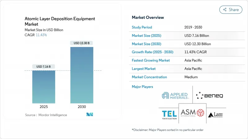
Atomic Layer Deposition Equipment - Market Share Analysis, Industry Trends & Statistics, Growth Forecasts (2025 - 2030)
The atomic layer deposition equipment market size stood at USD 7.16 billion in 2025 and is forecast to reach USD 12.30 billion by 2030, reflecting an 11.43% CAGR.
This expansion has been propelled by rising process intensity at advanced logic and 3-D memory nodes, adoption of gate-all-around (GAA) transistors, and fast-growing demand from solid-state battery and micro-LED lines. Asia-Pacific's large wafer-fab build-out, coupled with policy incentives in the United States and European Union, has enlarged the buyer base for single-wafer, batch, and spatial platforms. Equipment makers are capturing value by introducing high-throughput reactors, offering lower-resistance metal films such as ruthenium and molybdenum, and embedding real-time precursor-utilization analytics. Meanwhile, precursor scarcity, PFAS regulation, and the need to trim cost-per-wafer keep process integration and supply-chain resilience at centre stage for tool vendors and chipmakers alike.
Global Atomic Layer Deposition Equipment Market Trends and Insights
Surging 3-D NAND and DRAM Node Shrink in Asia
Layer counts already surpassed 200 in commercial 3-D NAND devices, requiring dozens of high-aspect-ratio dielectric and metal layers deposited with sub-Angstrom precision. Leading memory makers in South Korea and China ramped orders for thermal ALD reactors that can maintain thickness variation below 1% across structures with 100:1 aspect ratios. Memory price recovery in 2024-2025 restored fab utilization, raising tool demand even amid export-control headwinds. Chinese fabs purchased 40% of global wafer-fab equipment in 2024, creating a regional undersupply of ALD precursor capacity. Vendors able to couple batch economics with high-k dielectric uniformity won most replacement awards.
Transition to Gate-All-Around and High-k Metal Gate Logic
GAA architectures move the gate electrode around the entire nanoribbon, multiplying the number of conformal high-k/metal layers per device. TSMC's 2 nm platform, slated for 2H 2025 mass production, integrates hundreds of ALD steps to secure threshold-voltage control while shaving 25-30% power versus 3 nm nodes. Molybdenum and ruthenium ALD replaced tungsten and copper in several interconnect levels, trimming line resistance by 35% and simplifying CMP. Demand has skewed toward single-wafer tools with in-source metrology that validates film thickness after every cycle. Suppliers capable of delivering sub-2 A thickness repeatability at >200 Wph throughput are best positioned.
Scarcity and Cost Volatility of Precursor Metals
Ruthenium and iridium supply chains remained concentrated in two producing nations, exposing fabs to price swings above 40% in 2024. One leading-edge logic fab deferred a 3 nm ramp by three months owing to Ru shortages, adding precursor-recycling skids that raised tool CAPEX by 15%. Research into zinc-alkyl-assisted cobalt ALD cut sheet resistance to 15 µΩ cm but still trails Ru in electromigration life. Until alternative chemistries mature, the price of PGMs will cap aggressive cost-down roadmaps.
Other drivers and restraints analyzed in the detailed report include:
- Rapid Adoption of Mini/Micro-LED Backplanes
- EV Battery Solid-State Electrolyte Coatings Demand
- Throughput Limitations vs. High-Volume Foundry Targets
For complete list of drivers and restraints, kindly check the Table Of Contents.
Segment Analysis
Thermal ALD captured the largest slice of the atomic layer deposition equipment market at 55.2% in 2024. Single-wafer thermal reactors proved indispensable for high-aspect-ratio memory etch-stop layers, with recipe flexibility supporting frequent precursor swaps. However, spatial ALD's 17.1% CAGR makes it the standout gainer through 2030. A top OLED panel maker validated atmospheric spatial ALD encapsulation that quadrupled throughput and met stringent barrier metrics. The resulting cost per square meter fell by 28%, steering fresh orders toward in-line spatial tools. Plasma-enhanced ALD widened its appeal for flexible electronics, enabling sub-100 °C film growth critical for plastic substrates. Vendors also released roll-to-roll variants, pushing ALD into barrier films for food and solar modules.
The atomic layer deposition equipment market size for Spatial ALD is projected to expand faster than any other segment, driven by demand from display and solar fabs. Conversely, ALE-enabled platforms surfaced as an emerging niche; integrating deposition and etch within one frame shortens process queues for 232-layer NAND stair-etch steps. Collectively, these developments diversified revenue streams beyond the core semiconductor base.
Cluster systems held 65.2% of 2024 revenue, favored for recipe agility at sub-3 nm logic lines. A recent upgrade that combined advanced precursor-vapor delivery with machine-learning fault detection trimmed cycle time 25% and boosted wafer-to-wafer uniformity 40%. Such productivity gains helped sustain the atomic layer deposition equipment market share advantage of single-wafer tools.
Batch reactors, however, are staging a comeback as memory and analog fabs seek lower cost per wafer. New hot-wall designs process 100 wafers simultaneously while controlling temperature within +-1 °C. A South Korean memory producer realized 30% cost savings when migrating a dielectric liner step from cluster to batch ALD. Consequently, batch revenue is on pace for a 14.3% CAGR, outstripping overall market growth.
The Atomic Layer Deposition Equipment Market Report is Segmented by Equipment Type (Thermal ALD, and More), by Reactor Configuration (Cluster, Stand-Alone Batch), by Substrate Size (<= 200 Mm, and More), by Film Chemistry (Oxide Films, Nitride and Oxy-Nitride Films, and More), by Application (Semiconductor Logic and Memory, and More), by Geography (North America, South America, Europe, Asia-Pacific, and Middle East and Africa).
Geography Analysis
Asia-Pacific retained a 41.8% revenue share in 2024 and is forecast to post a 17.3% CAGR through 2030. Taiwan, South Korea, and China jointly produced more than 80% of global logic and memory wafers, ensuring concentrated tool demand. China alone bought 40% of all wafer-fab equipment in 2024 despite export curbs, underpinned by a USD 47 billion national fund. The region also hosts most micro-LED capacity, further amplifying spatial ALD adoption.
North America ranked second, buoyed by CHIPS and the Science Act incentives. New fabs in Arizona, Ohio, and Texas earmarked multi-billion-dollar ALD tool budgets for GAA pilot lines and advanced chiplet packaging. U.S. firms invested USD 107.5 billion in research and development and capex during 2023, reinforcing domestic demand.
Europe's share is smaller yet accelerating. The European Chips Act mobilized EUR 43 billion (USD 49.09 billion), including EUR 3.7 billion (USD 4.22 billion) for five pilot lines that rely on ALD to prototype advanced packaging stacks. Emerging activity in Brazil, Israel, and the United Arab Emirates broadened the customer map, mainly through research lines targeting power electronics and renewable-energy storage.
- ASM International N.V.
- Applied Materials Inc.
- Tokyo Electron Limited
- Lam Research Corporation
- Veeco Instruments Inc.
- Oxford Instruments plc
- Beneq Oy
- Picosun Oy
- Entegris Inc.
- Kurt J. Lesker Company
- Hitachi High-Tech Corporation
- Ulvac Inc.
- Aixtron SE
- SENTECH Instruments GmbH
- CVD Equipment Corporation
- Forge Nano Inc.
- ALD NanoSolutions Inc.
- Lotus Applied Technology
- LPE S.p.A.
- SVT Associates
- Arradiance LLC
- Beneq R2R (Service Business)
Additional Benefits:
- The market estimate (ME) sheet in Excel format
- 3 months of analyst support
TABLE OF CONTENTS
1 INTRODUCTION
- 1.1 Study Assumptions and Market Definition
- 1.2 Scope of the Study
2 RESEARCH METHODOLOGY
3 EXECUTIVE SUMMARY
4 MARKET LANDSCAPE
- 4.1 Market Overview
- 4.2 Market Drivers
- 4.2.1 Surging 3-D NAND and DRAM Node Shrink in Asia
- 4.2.2 Transition to Gate-All-Around (GAA) and High-K Metal Gate Logic
- 4.2.3 Rapid Adoption of Mini/Micro-LED Backplanes
- 4.2.4 EV Battery Solid-State Electrolyte Coatings Demand
- 4.2.5 Medical Implant Nano-Coatings for Improved Bio-compatibility
- 4.2.6 Government-funded Pilot-Line Investments (EU Chips Act, CHIPS and Science Act)
- 4.3 Market Restraints
- 4.3.1 Scarcity and Cost Volatility of Precursor Metals (Ru, Ir, Co)
- 4.3.2 Throughput Limitations vs. High-Volume Foundry Targets
- 4.3.3 Competing Spatial CVD for OLED Encapsulation
- 4.3.4 Stringent EHS Regulations on Fluorinated Plasma By-products
- 4.4 Value Chain Analysis
- 4.5 Regulatory and Technological Outlook
- 4.6 Porter's Five Forces
- 4.6.1 Bargaining Power of Suppliers
- 4.6.2 Bargaining Power of Buyers
- 4.6.3 Threat of New Entrants
- 4.6.4 Threat of Substitutes
- 4.6.5 Intensity of Competitive Rivalry
- 4.7 Impact of Macroeconomic Factors on the market
5 MARKET SIZE AND GROWTH FORECASTS (VALUE)
- 5.1 By Equipment Type
- 5.1.1 Thermal ALD (Batch)
- 5.1.2 Plasma-Enhanced ALD (PEALD)
- 5.1.3 Spatial ALD
- 5.1.4 Roll-to-Roll / Sheet-to-Sheet ALD
- 5.1.5 Atomic Layer Etching (ALE)-Enabled Tools
- 5.2 By Reactor Configuration
- 5.2.1 Cluster (Single-Wafer)
- 5.2.2 Stand-alone Batch
- 5.3 By Substrate Size
- 5.3.1 <= 200 mm
- 5.3.2 300 mm
- 5.3.3 >= 450 mm Pilot Lines
- 5.4 By Film Chemistry
- 5.4.1 Oxide Films
- 5.4.2 Nitride and Oxy-Nitride Films
- 5.4.3 Metal Films (Co, Ru, Ti, Al, Cu)
- 5.4.4 Fluoride and Sulfide Films
- 5.5 By Application
- 5.5.1 Semiconductor Logic and Memory
- 5.5.2 Advanced Packaging and Heterogeneous Integration
- 5.5.3 Power and Optoelectronics (SiC, GaN, LEDs)
- 5.5.4 Energy Devices (Li-ion, Solid-State, Fuel Cells)
- 5.5.5 Biomedical and Implant Surface Functionalization
- 5.5.6 Automotive Sensors and ADAS
- 5.6 By Geography
- 5.6.1 North America
- 5.6.1.1 United States
- 5.6.1.2 Canada
- 5.6.1.3 Mexico
- 5.6.2 South America
- 5.6.2.1 Brazil
- 5.6.2.2 Argentina
- 5.6.2.3 Rest of South America
- 5.6.3 Europe
- 5.6.3.1 Germany
- 5.6.3.2 United Kingdom
- 5.6.3.3 France
- 5.6.3.4 Italy
- 5.6.3.5 Spain
- 5.6.3.6 Russia
- 5.6.3.7 Rest of Europe
- 5.6.4 Asia-Pacific
- 5.6.4.1 China
- 5.6.4.2 Japan
- 5.6.4.3 India
- 5.6.4.4 South Korea
- 5.6.4.5 South-East Asia
- 5.6.4.6 Rest of Asia-Pacific
- 5.6.5 Middle East and Africa
- 5.6.5.1 Middle East
- 5.6.5.1.1 Saudi Arabia
- 5.6.5.1.2 United Arab Emirates
- 5.6.5.1.3 Turkey
- 5.6.5.1.4 Rest of Middle East
- 5.6.5.2 Africa
- 5.6.5.2.1 South Africa
- 5.6.5.2.2 Nigeria
- 5.6.5.2.3 Rest of Africa
- 5.6.1 North America
6 COMPETITIVE LANDSCAPE
- 6.1 Market Concentration
- 6.2 Strategic Initiatives and JV Analysis
- 6.3 Market Share Analysis
- 6.4 Company Profiles (includes Global-level Overview, Market-level Overview, Core Segments, Financials as available, Strategic Information, Market Rank/Share, Products and Services, Recent Developments)
- 6.4.1 ASM International N.V.
- 6.4.2 Applied Materials Inc.
- 6.4.3 Tokyo Electron Limited
- 6.4.4 Lam Research Corporation
- 6.4.5 Veeco Instruments Inc.
- 6.4.6 Oxford Instruments plc
- 6.4.7 Beneq Oy
- 6.4.8 Picosun Oy
- 6.4.9 Entegris Inc.
- 6.4.10 Kurt J. Lesker Company
- 6.4.11 Hitachi High-Tech Corporation
- 6.4.12 Ulvac Inc.
- 6.4.13 Aixtron SE
- 6.4.14 SENTECH Instruments GmbH
- 6.4.15 CVD Equipment Corporation
- 6.4.16 Forge Nano Inc.
- 6.4.17 ALD NanoSolutions Inc.
- 6.4.18 Lotus Applied Technology
- 6.4.19 LPE S.p.A.
- 6.4.20 SVT Associates
- 6.4.21 Arradiance LLC
- 6.4.22 Beneq R2R (Service Business)
7 MARKET OPPORTUNITIES AND FUTURE OUTLOOK
- 7.1 White-space and Unmet-Need Assessment

