
PUBLISHER: Mordor Intelligence | PRODUCT CODE: 1851086

PUBLISHER: Mordor Intelligence | PRODUCT CODE: 1851086
Substrate-Like-PCB - Market Share Analysis, Industry Trends & Statistics, Growth Forecasts (2025 - 2030)
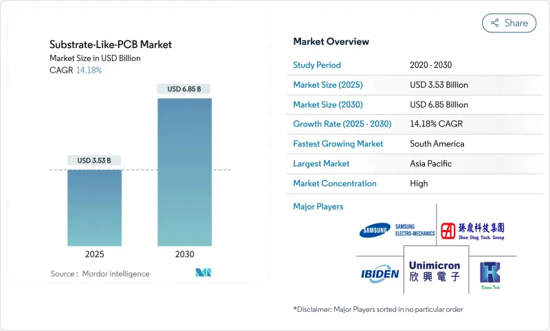
The Substrate-Like PCB market size reached USD 3.53 billion in 2025 and is forecast to advance to USD 6.85 billion by 2030, reflecting a 14.18% CAGR.
Demand accelerates as OEMs migrate from conventional high-density interconnect boards to solutions that deliver IC-substrate-level wiring density without fully moving into semiconductor packaging. Volume growth is anchored in 5G radio, artificial-intelligence processors, and automotive ADAS controllers that require <=25 µm line/space geometries for signal integrity. Asia-Pacific captured 69% of revenue in 2024, benefiting from tight linkages between semiconductor foundries and PCB fabricators plus sustained investment in modified semi-additive processing lines . ABF build-up films dominate material selection on the strength of low-loss dielectric properties, though their concentrated supply base prompts vertical-integration moves by tier-one fabricators. Yield optimization below 25 µm increasingly hinges on AI-enabled inspection, giving process-control leaders a structural cost advantage. Geopolitical reshoring incentives-such as the USD 30 million U.S. Department of Defense grant-add regional diversification while tightening qualification hurdles for new entrants.
Global Substrate-Like-PCB Market Trends and Insights
Surging smartphone OEM adoption for high-density interconnects
Premium handset vendors used Substrate-Like PCB market technology to raise circuit density by roughly 30%, unlocking more space for 5G modems, AI coprocessors, and multi-lens camera control while holding device thickness flat. Scale benefits from flagship models flow into mid-tier phones, sustaining high production runs that amortize capital costs across broader portfolios.
Rising demand for 5G communication modules
Millimeter-wave base-station boards and consumer 5G radio cards require <=25 µm routing to curb insertion loss and crosstalk. Network OEMs specify Substrate-Like PCB market designs for massive-MIMO arrays and beam-forming front ends, linking board density with spectral-efficiency targets. The same design rules migrate into smartphones and tablets as data-rate expectations climb.
High CAPEX for SLP production lines
A greenfield Substrate-Like PCB market line requires precision laser drills, direct-imaging photolithography, and Class 1000 cleanroom space. The USD 100 million outlay pressures smaller fabricators to form joint ventures or exit, consolidating capacity with incumbents that boast balance-sheet depth.
Other drivers and restraints analyzed in the detailed report include:
- Miniaturization trends in wearables & IoT devices
- Automotive ADAS & EV electronics escalating PCB complexity
- Process-yield challenges at <25 µm L/S
For complete list of drivers and restraints, kindly check the Table Of Contents.
Segment Analysis
Smartphones accounted for 47% of Substrate-Like PCB market revenue in 2024 and remain the anchor customer set entering 2025. The segment leverages the Substrate-Like PCB market size advantage inherent in global handset shipments to underwrite rapid capacity ramps. Premium devices that pair AI engines with 5-antenna 5G radios require <=25 µm wiring, reinforcing demand at the leading edge. A cascading cost curve then enables mid-tier adoption, extending volume visibility beyond flagship refreshes.
Wearables are the fastest-growing niche at a 15.4% CAGR, catalyzed by health monitoring mandates and augmented-reality headsets. Suppliers optimize energy density by embedding high-efficiency power-management ICs directly onto the board, proving the value of SLP's sub-0.5 mm via pitch. Automotive electronics add diversified revenue streams as OEMs specify redundant sensor-fusion boards. Networking infrastructure and edge-computing gateways adopt SLP to meet thermal and latency targets, while industrial and medical systems command premium ASPs due to stringent reliability.
The 10-12-layer cohort controlled 37% of 2024 output, balancing routing headroom with manageable yield risk. This stratum remains the workhorse for the Substrate-Like PCB market size tied to smartphone boards. Designs exceeding 12 layers are scaling at 13% CAGR on the back of chiplet-based AI accelerators and automotive domain controllers. Here, "Substrate-Like PCB market share" accrues to fabricators that master cumulative-warp control across sequential lamination cycles. Layer counts of 8-10 serve cost-sensitive consumer IoT products, offering an entry path for HDI vendors up-skilling toward SLP.
Substrate-Like-PCB Market is Segmented by Application (Smartphones, Tablets, Wearables, Automotive Electronics, and More), by Build-Up Layer Count (8 - 10 Layers, 10 - 12 Layers, and More), by Base Material (ABF, Modified Epoxy / FR-4, and More), by Line/Space Resolution (30/30 Mm, 25/25 Mm, and <= 20/20 Mm) and by Geography. The Market Forecasts are Provided in Terms of Value (USD).
Geography Analysis
Asia-Pacific retained a 69% revenue share in 2024, anchored by Taiwan, South Korea, and Japan. Foundry-adjacent ecosystems accelerate design-for-manufacture cycles, letting PCB vendors co-opt R&D from semiconductor customers. Chinese fabricators expand capacity aggressively; Zhen Ding booked 23% top-line growth in 2024 and is steering toward 50% CAGR in IC-substrate revenue through 2027. Material majors in Japan supply ABF films to the region, reinforcing local supply-chain density.
North America contributed 18% in 2024 but benefits from USD 30 million defense funding plus CHIPS Act incentives that defray advanced tooling. TTM Technologies' USD 130 million Syracuse facility constitutes the largest ultra-HDI investment on the continent, targeting secure-supply defense workloads. Automotive electrification and private-network 5G rollouts give regional demand a structural leg.
Europe's smaller yet strategic footprint is led by AT&S, which extended Malaysian production to serve German OEMs needing ADAS boards. EU grants targeting technology sovereignty support incremental SLP lines, especially for automotive and medical verticals.
South America, though starting from a low base, records a 12.2% CAGR as near-shoring shifts light assembly to the Dominican Republic and Mexico. Governments promote electronics clusters for job creation, drawing pilot SLP investment to align with free-trade agreements.
The Middle East and Africa remain nascent but preserve upside through sovereign diversification funds channeling capital into semiconductor back-end ecosystems, enabling future Substrate-Like PCB market penetration once regional design houses mature.
- Kinsus Interconnect Technology Corp.
- Ibiden Co., Ltd.
- Compeq Manufacturing Co., Ltd.
- Daeduck Electronics Co., Ltd.
- Unimicron Technology Corp.
- Zhen Ding Technology Holding
- TTM Technologies
- Meiko Electronics Co., Ltd.
- ATandS AG
- Korea Circuit Co., Ltd.
- LG Innotek Co., Ltd.
- Samsung Electro-Mechanics
- Shennan Circuits Co., Ltd.
- Tripod Technology
- Fujitsu Interconnect
- Wus Printed Circuit
- HannStar Board Corp.
- Nippon Mektron Ltd.
- NCAB Group AB
- Multek Ltd.
Additional Benefits:
- The market estimate (ME) sheet in Excel format
- 3 months of analyst support
TABLE OF CONTENTS
1 INTRODUCTION
- 1.1 Study Assumptions and Market Definition
- 1.2 Scope of the Study
2 RESEARCH METHODOLOGY
3 EXECUTIVE SUMMARY
4 MARKET LANDSCAPE
- 4.1 Market Overview
- 4.2 Market Drivers
- 4.2.1 Surging smartphone OEM adoption for high-density interconnects
- 4.2.2 Rising demand for 5G communication modules
- 4.2.3 Miniaturization trends in wearables and IoT devices
- 4.2.4 Automotive ADAS and EV electronics escalating PCB complexity
- 4.2.5 Flip-chip on SLP enabling heterogeneous integration
- 4.2.6 Government subsidies for on-shore advanced PCB fabs
- 4.3 Market Restraints
- 4.3.1 High CAPEX for SLP production lines
- 4.3.2 Process-yield challenges at <25 m L/S
- 4.3.3 Environmental rules on specialty build-up chemistries
- 4.3.4 Supply risk of ABF resin due to limited vendors
- 4.4 Value / Supply-Chain Analysis
- 4.5 Regulatory Landscape
- 4.6 Technological Outlook
- 4.7 Porters Five Forces
- 4.7.1 Bargaining Power of Suppliers
- 4.7.2 Bargaining Power of Buyers
- 4.7.3 Threat of New Entrants
- 4.7.4 Threat of Substitutes
- 4.7.5 Intensity of Rivalry
- 4.8 Industry Value Chain Analysis
5 MARKET SIZE and GROWTH FORECASTS (VALUE)
- 5.1 By Application
- 5.1.1 Smartphones
- 5.1.2 Tablets
- 5.1.3 Wearables
- 5.1.4 Automotive Electronics
- 5.1.5 Networking and Communication Infrastructure
- 5.1.6 IoT / Edge Devices
- 5.1.7 Industrial and Medical Electronics
- 5.2 By Build-Up Layer Count
- 5.2.1 8 - 10 Layers
- 5.2.2 10 - 12 Layers
- 5.2.3 > 12 Layers
- 5.3 By Base Material
- 5.3.1 ABF (Ajinomoto Build-up Film)
- 5.3.2 Modified Epoxy / FR-4
- 5.3.3 Others (PTFE, BT Resin)
- 5.4 By Line/Space Resolution
- 5.4.1 30 / 30 µm
- 5.4.2 25 / 25 µm
- 5.4.3 20 / 20 µm
- 5.5 By Geography
- 5.5.1 North America
- 5.5.1.1 United States
- 5.5.1.2 Canada
- 5.5.1.3 Mexico
- 5.5.2 South America
- 5.5.2.1 Brazil
- 5.5.2.2 Argentina
- 5.5.2.3 Rest of South America
- 5.5.3 Europe
- 5.5.3.1 United Kingdom
- 5.5.3.2 Germany
- 5.5.3.3 France
- 5.5.3.4 Italy
- 5.5.3.5 Spain
- 5.5.3.6 Russia
- 5.5.3.7 Rest of Europe
- 5.5.4 APAC
- 5.5.4.1 China
- 5.5.4.2 Japan
- 5.5.4.3 South Korea
- 5.5.4.4 India
- 5.5.4.5 Australia
- 5.5.4.6 Rest of APAC
- 5.5.5 Middle East and Africa
- 5.5.5.1 GCC
- 5.5.5.2 South Africa
- 5.5.5.3 Rest of Middle East and Africa
- 5.5.1 North America
6 COMPETITIVE LANDSCAPE
- 6.1 Market Concentration
- 6.2 Strategic Moves
- 6.3 Market Share Analysis
- 6.4 Company Profiles (includes Global level Overview, Market level overview, Core Segments, Financials as available, Strategic Information, Market Rank/Share for key companies, Products and Services, and Recent Developments)
- 6.4.1 Kinsus Interconnect Technology Corp.
- 6.4.2 Ibiden Co., Ltd.
- 6.4.3 Compeq Manufacturing Co., Ltd.
- 6.4.4 Daeduck Electronics Co., Ltd.
- 6.4.5 Unimicron Technology Corp.
- 6.4.6 Zhen Ding Technology Holding
- 6.4.7 TTM Technologies
- 6.4.8 Meiko Electronics Co., Ltd.
- 6.4.9 ATandS AG
- 6.4.10 Korea Circuit Co., Ltd.
- 6.4.11 LG Innotek Co., Ltd.
- 6.4.12 Samsung Electro-Mechanics
- 6.4.13 Shennan Circuits Co., Ltd.
- 6.4.14 Tripod Technology
- 6.4.15 Fujitsu Interconnect
- 6.4.16 Wus Printed Circuit
- 6.4.17 HannStar Board Corp.
- 6.4.18 Nippon Mektron Ltd.
- 6.4.19 NCAB Group AB
- 6.4.20 Multek Ltd.
7 MARKET OPPORTUNITIES and FUTURE OUTLOOK
- 7.1 White-space and Unmet-Need Assessment

