
PUBLISHER: Mordor Intelligence | PRODUCT CODE: 1851511

PUBLISHER: Mordor Intelligence | PRODUCT CODE: 1851511
Flip Chip Technology - Market Share Analysis, Industry Trends & Statistics, Growth Forecasts (2025 - 2030)
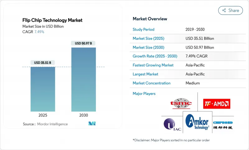
The flip chip technology market size stood at USD 35.51 billion in 2025 and is on track to reach USD 50.97 billion by 2030, reflecting a 7.49% CAGR.
Growth mirrored the semiconductor industry's transition to chiplet-based architectures that required dense, thermally efficient interconnects. AI data-center build-outs pushed high-bandwidth memory packaging to the fore, while copper-pillar and hybrid bonding lines addressed the fine-pitch needs that traditional solder bumps could not meet. Foundries entered the packaging arena, accelerating vertical integration and bringing new competitive pressures on outsourced assembly and test providers. Asia-Pacific retained scale advantages, yet supply-chain de-risking programs in North America and Europe triggered large green-field investments in advanced packaging facilities.
Global Flip Chip Technology Market Trends and Insights
Surge in Heterogeneous Integration Demand (AI/HPC)
Chipmakers pivoted from 2D scaling to heterogeneous integration that joined multiple chiplets in a single package, lifting demand for fine-pitch Cu-to-Cu interconnects. TSMC's plan to boost CoWoS capacity to 1.31 million units by 2026 illustrated how GPU vendors such as Nvidia shaped the flip chip technology market. The approach enhanced bandwidth while lowering power compared with legacy bumps, supporting the performance roadmap for AI accelerators.
Rising Adoption of Copper-Pillar and Micro-Bump Interconnects
Copper-pillar bumps delivered superior electrical resistance and reliability, explaining their 46.3% 2024 revenue share. High-speed plating chemistries from DuPont provided uniform thickness control essential for sub-40 µm pitches. The shift eroded tin-lead dominance and paved the way for 3D integration schemes that underpin the flip chip technology market.
High Capital Intensity of Advanced Bumping Lines
Scaling to sub-10 µm pitches required lithography steppers, advanced sputter tools, and plasma cleaners that pushed line cost above USD 250 million per module. TSMC earmarked USD 90 billion for dedicated packaging plants, underscoring the entry hurdle for smaller competitors. Collaborative R&D programs such as 3M's participation in the US-JOINT consortium aimed to spread risk across the supply chain.
Other drivers and restraints analyzed in the detailed report include:
- Wearables and IoT Miniaturization Push
- Automotive ADAS/EV Reliability Requirements
- Lead-Free Reliability and Warpage Challenges
For complete list of drivers and restraints, kindly check the Table Of Contents.
Segment Analysis
Copper pillar technology held 46.3% revenue in 2024 within the flip chip technology market. The segment benefited from reduced resistance and heightened current-carrying capability. The flip chip technology market size for Cu-to-Cu hybrid bonding is projected to expand at a 9.8% CAGR as chiplet adoption grows. The hybrid method lowered inter-chip spacing to 0.8 µm, far beyond solder's physical limits. Tin-lead solutions still served legacy nodes, whereas gold-stud bumps remained confined to aerospace.
Advances in electroplated chemistries sustained pillar height uniformity below 2%, a prerequisite for 3D stacks. IEEE research validated solder-free Cu-Cu bonding at 260 °C as a manufacturable path for heterogeneous integration. Innovations positioned copper formats to absorb share from both lead-free and precious-metal alternatives.
FC-BGA commanded 38.1% of 2024 revenue thanks to proven reliability in servers. Fan-out WLP and panel-level formats are expected to record a 10.1% CAGR, catalyzed by AI accelerators demanding large body sizes. ASE allocated USD 200 million to 310 mm X 310 mm panels that promise sevenfold usable area over wafers, a cost breakthrough. The flip chip technology market size for panel-level packages will climb as line yields improve.
Specialty flows such as CoWoS and EMIB enable HBM stacking essential for AI training units. IBM and Intel pursued glass-substrate roadmaps that offer lower warpage and higher line-space ratios than organic laminates. 3D IC with TSV remained a niche for extreme bandwidth-class devices due to high cost and process complexity, but set the ceiling on attainable performance.
Flip Chip Technology Market is Segmented by Wafer Bumping Process (Copper Pillar, Tin-Lead Eutectic Solder, and More), Packaging Technology (FC-BGA, FCCSP/CSP, and More), Product (Memory, CMOS Image Sensor, and More), End-Use Industry (Consumer Electronics and Wearables, Automotive and Transportation, Industrial and Robotics, and More), and Geography (North America, South America, Europe, Asia-Pacific, and Middle East and Africa).
Geography Analysis
Asia-Pacific held 54.5% of 2024 revenue. The region housed the bulk of wafer fabs and retained cost advantages, sustaining the largest slice of the flip chip technology market. Government incentives supported next-node R&D, yet export-control actions induced leading firms to build parallel capacity offshore. North America accelerated foundry and packaging startups under the CHIPS Act, adding resilience and creating a local demand pull. The flip chip technology market share for North America is expected to rise modestly as Arizona and Texas campuses come online.
Europe pursued technology sovereignty through the European Chips Act and directed capital toward panel-level and glass-core substrate lines. Silicon Box's Novara facility is slated to process 10,000 panels weekly by 2028, anchoring a regional ecosystem. Middle East and Africa remained early-stage but benefited from electronics final-assembly hubs that feed into global supply chains.
Supply-chain diversification scattered future investments across at least three continents, muting single-region dominance. However, Asia-Pacific still boasted unmatched engineering depth, keeping it the reference center for high-volume manufacturing.
- Amkor Technology, Inc.
- ASE Technology Holding Co., Ltd.
- Taiwan Semiconductor Manufacturing Company Limited
- Jiangsu Changjiang Electronics Technology Co., Ltd.
- Powertech Technology Inc.
- Chipbond Technology Corporation
- UTAC Holdings Ltd.
- TF-AMD Microelectronics Sdn. Bhd.
- Shinko Electric Industries Co., Ltd.
- Unisem (M) Berhad
- Hana Micron Inc.
- Nepes Corporation
- Carsem (M) Sdn. Bhd.
- Sigurd Microelectronics Corporation
- AT&S Austria Technologie & Systemtechnik AG
- Intel Corporation
- Samsung Electronics Co., Ltd.
- Advanced Micro Devices, Inc.
- Texas Instruments Incorporated
- United Microelectronics Corporation
- STATS ChipPAC Pte. Ltd.
- SFA Semicon Co., Ltd.
- Tongfu Microelectronics Co., Ltd.
- Huatian Technology Co., Ltd.
- Lingsen Precision Industries, Ltd.
Additional Benefits:
- The market estimate (ME) sheet in Excel format
- 3 months of analyst support
TABLE OF CONTENTS
1 INTRODUCTION
- 1.1 Study Assumptions and Market Definition
- 1.2 Scope of the Study
2 RESEARCH METHODOLOGY
3 EXECUTIVE SUMMARY
4 MARKET LANDSCAPE
- 4.1 Market Overview
- 4.2 Market Drivers
- 4.2.1 Surge in heterogeneous integration demand (AI/ HPC)
- 4.2.2 Rising adoption of copper-pillar and micro-bump interconnects
- 4.2.3 Wearables and IoT miniaturization push
- 4.2.4 Automotive ADAS/EV reliability requirements
- 4.2.5 Glass-core substrate commercial trials
- 4.2.6 Demand for chip-let-ready Cu-to-Cu hybrid bonding
- 4.3 Market Restraints
- 4.3.1 High capital intensity of advanced bumping lines
- 4.3.2 Lead-free reliability and warpage challenges
- 4.3.3 Sub-10 µm alignment yield losses
- 4.3.4 Supply-chain exposure to critical metal chemicals
- 4.4 Value Chain Analysis
- 4.5 Impact of Macroeconomic Factors
- 4.6 Regulatory Landscape
- 4.7 Technological Outlook
- 4.8 Porter's Five Forces
- 4.8.1 Bargaining Power of Suppliers
- 4.8.2 Bargaining Power of Buyers
- 4.8.3 Threat of New Entrants
- 4.8.4 Threat of Substitutes
- 4.8.5 Intensity of Competitive Rivalry
- 4.9 Investment Analysis
5 MARKET SIZE AND GROWTH FORECASTS (VALUE)
- 5.1 By Wafer Bumping Process
- 5.1.1 Copper Pillar
- 5.1.2 Tin-Lead Eutectic Solder
- 5.1.3 Lead-Free Solder (SnAg, SAC, etc.)
- 5.1.4 Gold-Stud Bumping
- 5.1.5 Cu-to-Cu Hybrid / Direct Bond
- 5.2 By Packaging Technology
- 5.2.1 FC-BGA (2D/2.1D/2.5D/3D)
- 5.2.2 FCCSP / CSP
- 5.2.3 CoWoS / InFO / EMIB
- 5.2.4 Fan-Out WLP / PLP
- 5.2.5 3D IC with TSV
- 5.3 By Product
- 5.3.1 Memory (DRAM, HBM)
- 5.3.2 CMOS Image Sensor
- 5.3.3 LED and Mini/Micro-LED
- 5.3.4 SoC / Application Processor
- 5.3.5 GPU / AI Accelerator
- 5.3.6 CPU / Server Processor
- 5.4 By End-Use Industry
- 5.4.1 Consumer Electronics and Wearables
- 5.4.2 Automotive and Transportation
- 5.4.3 Industrial and Robotics
- 5.4.4 Telecommunications and 5G Infrastructure
- 5.4.5 Data Center and Cloud
- 5.4.6 Military and Aerospace
- 5.4.7 Medical and Healthcare Devices
- 5.5 By Geography
- 5.5.1 North America
- 5.5.1.1 United States
- 5.5.1.2 Canada
- 5.5.1.3 Mexico
- 5.5.2 South America
- 5.5.2.1 Brazil
- 5.5.2.2 Rest of South America
- 5.5.3 Europe
- 5.5.3.1 Germany
- 5.5.3.2 France
- 5.5.3.3 United Kingdom
- 5.5.3.4 Russia
- 5.5.3.5 Rest of Europe
- 5.5.4 Asia-Pacific
- 5.5.4.1 China
- 5.5.4.2 Taiwan
- 5.5.4.3 South Korea
- 5.5.4.4 Japan
- 5.5.4.5 Malaysia
- 5.5.4.6 Singapore
- 5.5.4.7 Rest of Asia-Pacific
- 5.5.5 Middle East and Africa
- 5.5.5.1 Middle East
- 5.5.5.1.1 Turkey
- 5.5.5.1.2 Rest of Middle East
- 5.5.5.2 Africa
- 5.5.5.2.1 South Africa
- 5.5.5.2.2 Rest of Africa
- 5.5.1 North America
6 COMPETITIVE LANDSCAPE
- 6.1 Market Concentration
- 6.2 Strategic Moves (M&A, JV, Capacity Expansions)
- 6.3 Market Share Analysis
- 6.4 Company Profiles (includes Global-level Overview, Market-level Overview, Core Segments, Financials, Strategic Information, Market Rank/Share, Products and Services, Recent Developments)
- 6.4.1 Amkor Technology, Inc.
- 6.4.2 ASE Technology Holding Co., Ltd.
- 6.4.3 Taiwan Semiconductor Manufacturing Company Limited
- 6.4.4 Jiangsu Changjiang Electronics Technology Co., Ltd.
- 6.4.5 Powertech Technology Inc.
- 6.4.6 Chipbond Technology Corporation
- 6.4.7 UTAC Holdings Ltd.
- 6.4.8 TF-AMD Microelectronics Sdn. Bhd.
- 6.4.9 Shinko Electric Industries Co., Ltd.
- 6.4.10 Unisem (M) Berhad
- 6.4.11 Hana Micron Inc.
- 6.4.12 Nepes Corporation
- 6.4.13 Carsem (M) Sdn. Bhd.
- 6.4.14 Sigurd Microelectronics Corporation
- 6.4.15 AT&S Austria Technologie & Systemtechnik AG
- 6.4.16 Intel Corporation
- 6.4.17 Samsung Electronics Co., Ltd.
- 6.4.18 Advanced Micro Devices, Inc.
- 6.4.19 Texas Instruments Incorporated
- 6.4.20 United Microelectronics Corporation
- 6.4.21 STATS ChipPAC Pte. Ltd.
- 6.4.22 SFA Semicon Co., Ltd.
- 6.4.23 Tongfu Microelectronics Co., Ltd.
- 6.4.24 Huatian Technology Co., Ltd.
- 6.4.25 Lingsen Precision Industries, Ltd.
7 MARKET OPPORTUNITIES AND FUTURE OUTLOOK
- 7.1 White-space and Unmet-Need Assessment

