
PUBLISHER: Mordor Intelligence | PRODUCT CODE: 1851578

PUBLISHER: Mordor Intelligence | PRODUCT CODE: 1851578
Photonic Integrated Circuit - Market Share Analysis, Industry Trends & Statistics, Growth Forecasts (2025 - 2030)
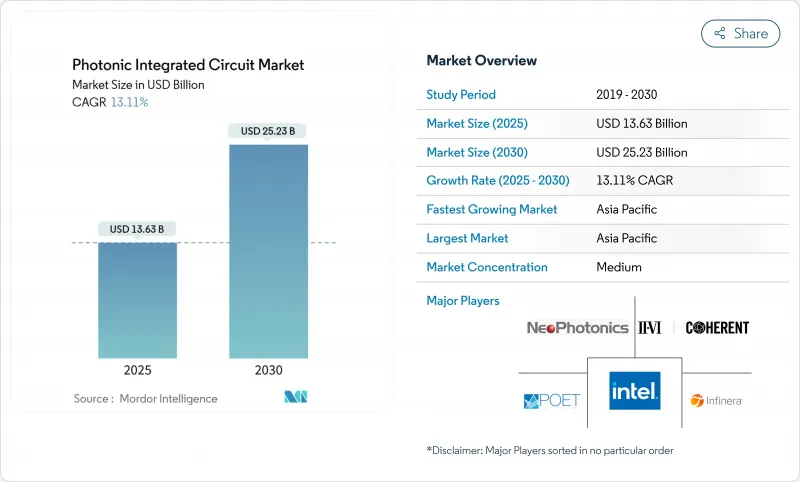
The photonic integrated circuit market size stood at USD 13.63 billion in 2025 and is projected to reach USD 25.23 billion by 2030, reflecting a 13.11% CAGR.
This expansion mirrored the shift from experimental silicon photonics toward production-scale deployment in data centers, telecom networks, and early quantum systems, as rising AI workloads exposed the bandwidth and energy limits of copper interconnects. Commercial momentum benefited from cost advantages gained by leveraging established CMOS fabs, a vibrant venture capital pipeline, and growing government incentives to localize advanced photonic manufacturing. Meanwhile, rapid progress in co-packaged optics, thin-film lithium niobate modulators, and heterogeneous InP/silicon laser integration widened the performance gap with legacy optics. Intensifying supply-chain risks around gallium and germanium highlighted the strategic value of diversified materials platforms and regional foundry footprints.
Global Photonic Integrated Circuit Market Trends and Insights
Silicon-Photonics Adoption in >400 G Data-Center Transceivers
North American hyperscale operators transitioned to 400 G and 800 G optical links to curb latency and power in AI clusters. Coherent Corp demonstrated a 1.6 T-DR8 module that cut energy per bit by more than 20% versus conventional pluggables. NVIDIA's Spectrum-X switch roadmap adopted co-packaged optics that delivered 30% power savings and 1.6 Tb/s port speeds. Such architectures integrate photonic engines beside switch ASICs, eliminating electrical ingress losses and setting a volume pathway through established 300 mm CMOS lines. Growing demand for multi-rack GPU fabrics positions silicon photonics as an indispensable element of next-generation AI infrastructure.
EU Pilot-Line Funding Catalysing Local PIC Foundries
The EUR 380 million (USD 447.30 million) Chips JU award to the PIXEurope consortium underpinned Europe's bid for photonic sovereignty. Pilot lines in Eindhoven and Enschede will offer open-access silicon and silicon-nitride runs, enabling SMEs to prototype without owning fabs. Projects such as photonixFAB focus on heterogeneous laser attachment at wafer scale, positioning Europe to meet local telecom and automotive demand when volume ramps after 2026. The initiative contrasts with vertically integrated US and Asian peers, promising a distributed, resilient supply chain.
Wafer-Scale Yield Challenges for InP PICs
Scaling InP wafers beyond 4 inches, strained defect control, and pushing up the cost per die. Coherent Corp's six-inch line quadrupled theoretical die count yet required new epitaxy and metrology processes to maintain yield. Fraunhofer ISE demonstrated InP-on-GaAs substrates that cut cost by 80% and opened a roadmap to eight-inch scaling. Persistent yield drag continued to limit InP competitiveness in cost-sensitive applications, dampening near-term growth.
Other drivers and restraints analyzed in the detailed report include:
- PIC-Enabled Coherent 5G Backhaul Roll-outs
- Solid-State LiDAR Cost Downs in Autonomous Vehicles
- Fragmented EDA Toolchain Prolonging Design Cycles
For complete list of drivers and restraints, kindly check the Table Of Contents.
Segment Analysis
The photonic integrated circuit market size associated with raw-material sales reached USD 4.93 billion in 2025, and silicon retained 37.4% of the photonic integrated circuit market share in 2024. A broad installed CMOS base sustained its lead for passive waveguides and cost-critical datacom parts. Yet silicon nitride deliveries rose at a 15.4% CAGR thanks to low propagation loss and wide transparency that suited lab-on-chip and quantum photonics. Indium phosphide stayed essential for high-power lasers, while gallium arsenide gained traction through heterogeneous laser bonding that simplified silicon light-source integration.
Competition between scalability and performance shaped vendor roadmaps. Healthcare startups selected silicon-nitride biocompatibility for point-of-care diagnostics, whereas long-haul telecom vendors adhered to InP modulators for 140 Gbaud links. HyperLight's USD 37 million raise to advance thin-film lithium-niobate modulators highlighted renewed interest in electro-optic champions. Increasing multilayer wafer stacking signalled a future where mixed materials co-reside on a single reticle, blurring traditional platform boundaries.
Component revenue surpassed USD 3 billion in 2025, with lasers accounting for 26.3% that year. Optical switch matrices outpaced all other devices at a 14.1% CAGR, reflecting demand for fully reconfigurable fabrics inside AI data-center clusters. Lumentum's 400 Gb/s-per-lane electro-absorption modulated laser exemplified cresting performance benchmarks.
Integrated light generation remained the linchpin of total cost. Foundries coupled InP or GaAs gain media onto silicon to curtail external laser packaging, but thermal and yield issues added complexity. Photodetectors and modulators benefited from thin-film lithium-niobate architectures that combined >= 100 GHz bandwidth with sub-1 V drive efficiency. Variable optical attenuators and wavelength demultiplexers matured, yet rising channel counts spurred miniaturized array implementations.
Photonic Integrated Circuit is Segmented by Raw Material (InP, Si, Sin, Gaas, Linbo3, and More), Component (Lasers, Modulators, Photodetectors, Filters, Switches, Amplifiers, and More), Integration Process (Hybrid, Monolithic, and More), Application (Telecommunications, Data Centers, Biomedical and Life-Sciences, and More), End-User (Telecom Service Providers, Cloud and Hyperscale Data-Center Operators, and More), and Geography.
Geography Analysis
North America generated the largest regional revenue share in 2024, of 35.4% of global sales 2024. Massive hyperscale data centers and CHIPS-Act incentives drew over USD 700 million of new silicon-photonics capex to Malta, New York. Venture rounds for quantum and AI photonics, such as Lightsynq's USD 18 million seed, fortified a vibrant start-up pipeline. However, reliance on Chinese gallium and germanium exposed material price shocks that climbed 75%-250% after 2024 export controls.
Asia-Pacific posted the fastest 16.5% CAGR as policymakers targeted photonic self-reliance. China subsidized CNY 8.2 billion (USD 1.15 billion) for integrated laser-silicon programs. Japan invested USD 305 million with Intel for optical semiconductors that cut data-center power use. Regional fabs produced six-inch thin-film lithium-niobate wafers that closed earlier Western technology gaps.
Europe combined open-access foundries with targeted M&A to sustain a 6.5% manufacturing CAGR from 2019-2024. The photonic integrated circuit market size for Europe was USD 3.02 billion in 2025. Sivers Photonics collaborated on narrow-linewidth tunable lasers to serve coherent modules, while Nokia's USD 2.3 billion Infinera deal consolidated continental optical competence. The region's emphasis on sovereignty and SME enablement diversified global supply and reduced overdependence on single-node manufacturing geographies.
- Infinera Corporation
- Lumentum Holdings Inc.
- Intel Corporation
- Coherent Corp. (II-VI)
- Cisco Systems Inc. (Acacia)
- NeoPhotonics Corporation
- POET Technologies Inc.
- EFFECT Photonics
- Celestial AI
- Source Photonics Inc.
- Sicoya GmbH
- HyperLight Corp
- Ayar Labs Inc.
- Lightmatter Inc.
- Marvell Technology
- Ligentec SA
- Xanadu Quantum Tech. Inc.
- Ciena Corporation
- OpenLight Photonic Inc.
- Juniper Networks (Aurrion IP)
Additional Benefits:
- The market estimate (ME) sheet in Excel format
- 3 months of analyst support
TABLE OF CONTENTS
1 INTRODUCTION
- 1.1 Study Assumptions and Market Definition
- 1.2 Scope of the Study
2 RESEARCH METHODOLOGY
3 EXECUTIVE SUMMARY
4 MARKET LANDSCAPE
- 4.1 Market Overview
- 4.2 Market Drivers
- 4.2.1 Silicon-Photonics Adoption in >400 G Data-Center Transceivers (North America)
- 4.2.2 EU Pilot-Line Funding Catalysing Local PIC Foundries
- 4.2.3 PIC-Enabled Coherent 5G Backhaul Roll-outs (Asia)
- 4.2.4 Solid-State LiDAR Cost Downs in Autonomous Vehicles
- 4.2.5 Venture Capital for Quantum-Interconnect PICs
- 4.2.6 Lab-on-Chip Photonic Diagnostics for Rapid Testing
- 4.3 Market Restraints
- 4.3.1 Wafer-Scale Yield Challenges for InP PICs
- 4.3.2 Fragmented EDA Toolchain Prolonging Design Cycles
- 4.3.3 On-Chip Laser Thermal-Management Limitations
- 4.3.4 Concentrated Foundry Supply and Geopolitical Exposure
- 4.4 Value Chain Analysis
- 4.5 Regulatory and Standards Landscape
- 4.6 Technological Roadmap and Manufacturing Process Analysis
- 4.7 Porter's Five Forces Analysis
- 4.7.1 Bargaining Power of Suppliers
- 4.7.2 Bargaining Power of Buyers
- 4.7.3 Threat of New Entrants
- 4.7.4 Intensity of Competitive Rivalry
- 4.7.5 Threat of Substitute Products
- 4.8 Macroeconomic Impact Assessment
- 4.9 Investment Analysis
5 MARKET SIZE AND GROWTH FORECASTS (VALUE)
- 5.1 By Raw Material
- 5.1.1 Indium Phosphide (InP)
- 5.1.2 Silicon (Si)
- 5.1.3 Silicon Nitride (SiN)
- 5.1.4 Gallium Arsenide (GaAs)
- 5.1.5 Lithium Niobate (LiNbO3)
- 5.1.6 Silica-on-Silicon
- 5.1.7 Other Materials (Polymer, PLC, etc.)
- 5.2 By Component
- 5.2.1 Lasers
- 5.2.2 Modulators
- 5.2.3 Photodetectors
- 5.2.4 Filters
- 5.2.5 Switches
- 5.2.6 Amplifiers
- 5.2.7 Multiplexers and Demultiplexers
- 5.2.8 Attenuators and VOA
- 5.2.9 Other Components
- 5.3 By Integration Process
- 5.3.1 Hybrid Integration
- 5.3.2 Monolithic Integration
- 5.3.3 Module-based/Subsystem Integration
- 5.4 By Application
- 5.4.1 Telecommunications (Long-haul and Metro)
- 5.4.2 Data Centers (Short-Reach and HPC Interconnects)
- 5.4.3 Biomedical and Life-Sciences
- 5.4.4 Optical Sensors and LiDAR
- 5.4.5 Metrology and Test/Measurement
- 5.4.6 Quantum Computing and Quantum Photonics
- 5.5 By End-user Industry
- 5.5.1 Telecom Service Providers
- 5.5.2 Cloud and Hyperscale Data-Center Operators
- 5.5.3 Healthcare and Diagnostics Companies
- 5.5.4 Automotive and Mobility OEMs
- 5.5.5 Industrial and Manufacturing
- 5.5.6 Defense and Aerospace
- 5.5.7 Research and Academia
- 5.6 By Geography
- 5.6.1 North America
- 5.6.1.1 United States
- 5.6.1.2 Canada
- 5.6.1.3 Mexico
- 5.6.2 Europe
- 5.6.2.1 Germany
- 5.6.2.2 France
- 5.6.2.3 United Kingdom
- 5.6.2.4 Nordics
- 5.6.2.5 Rest of Europe
- 5.6.3 Asia-Pacific
- 5.6.3.1 China
- 5.6.3.2 Taiwan
- 5.6.3.3 South Korea
- 5.6.3.4 Japan
- 5.6.3.5 India
- 5.6.3.6 Rest of Asia-Pacific
- 5.6.4 South America
- 5.6.4.1 Brazil
- 5.6.4.2 Mexico
- 5.6.4.3 Argentina
- 5.6.4.4 Rest of South America
- 5.6.5 Middle East and Africa
- 5.6.5.1 Middle East
- 5.6.5.1.1 Saudi Arabia
- 5.6.5.1.2 United Arab Emirates
- 5.6.5.1.3 Turkey
- 5.6.5.1.4 Rest of Middle East
- 5.6.5.2 Africa
- 5.6.5.2.1 South Africa
- 5.6.5.2.2 Rest of Africa
- 5.6.1 North America
6 COMPETITIVE LANDSCAPE
- 6.1 Market Concentration
- 6.2 Strategic Moves and Deal Flow
- 6.3 Market Share Analysis
- 6.4 Company Profiles (includes Global overview, Market overview, Core Segments, Financials, Strategic Information, Market Rank/Share, Products and Services, Recent Developments)
- 6.4.1 Infinera Corporation
- 6.4.2 Lumentum Holdings Inc.
- 6.4.3 Intel Corporation
- 6.4.4 Coherent Corp. (II-VI)
- 6.4.5 Cisco Systems Inc. (Acacia)
- 6.4.6 NeoPhotonics Corporation
- 6.4.7 POET Technologies Inc.
- 6.4.8 EFFECT Photonics
- 6.4.9 Celestial AI
- 6.4.10 Source Photonics Inc.
- 6.4.11 Sicoya GmbH
- 6.4.12 HyperLight Corp
- 6.4.13 Ayar Labs Inc.
- 6.4.14 Lightmatter Inc.
- 6.4.15 Marvell Technology
- 6.4.16 Ligentec SA
- 6.4.17 Xanadu Quantum Tech. Inc.
- 6.4.18 Ciena Corporation
- 6.4.19 OpenLight Photonic Inc.
- 6.4.20 Juniper Networks (Aurrion IP)
7 MARKET OPPORTUNITIES AND FUTURE OUTLOOK
- 7.1 White-space and Unmet-Need Assessment

