
PUBLISHER: Mordor Intelligence | PRODUCT CODE: 1906136

PUBLISHER: Mordor Intelligence | PRODUCT CODE: 1906136
Photoresist - Market Share Analysis, Industry Trends & Statistics, Growth Forecasts (2026 - 2031)
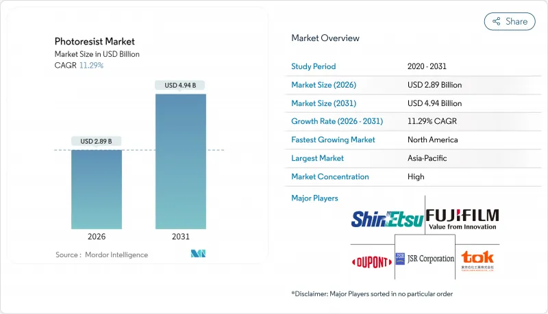
The Photoresist Market was valued at USD 2.60 billion in 2025 and estimated to grow from USD 2.89 billion in 2026 to reach USD 4.94 billion by 2031, at a CAGR of 11.29% during the forecast period (2026-2031).
The widespread deployment of extreme-ultraviolet (EUV) lithography at sub-10-nanometer dimensions, the fast-growing demand for artificial-intelligence (AI) accelerators, and government-funded fab incentives underpin this expansion. Semiconductor manufacturers in Taiwan, South Korea, and the United States are increasingly favoring metal-oxide and dry photoresists that deliver higher EUV absorption and lower line-edge roughness, thereby boosting throughput and reducing per-layer resist usage. Parallel momentum in 5G and Internet-of-Things (IoT) devices sustains demand for mature-node G-line, I-line, and KrF materials. Meanwhile, advanced packaging architectures-such as chiplets, fan-out wafer-level packaging, and co-packaged optics-require thick-film resists that are compatible with copper pillar and through-silicon-via (TSV) structures. Supply-chain risks remain elevated because three Japanese suppliers collectively account for roughly 60% of advanced resists, prompting regional diversification and localized capacity additions in North America and Europe.
Global Photoresist Market Trends and Insights
Growing Demand from Semiconductor and AI Accelerators
Chipmakers producing hardware for training large language models and powering inference workloads now pattern multiple redistribution layers, interposers, and TSVs for each device. NVIDIA's H100 and forthcoming Blackwell series adopt chiplet layouts that consume three to five times more photoresist per finished part than previous monolithic GPUs. Taiwan Semiconductor Manufacturing Company's (TSMC) expansion of CoWoS capacity lifts thick-film resist of up to 50 µm, while advanced copper pillar plating uses negative-tone formulations optimized for aspect ratios above 3:1. Volume gains occur first in Taiwan and South Korea but ripple into new fabs in the United States by 2027.
Accelerated EUV Lithography Adoption and High-NA Roadmap
ASML's 0.55-NA EUV scanners enable single-exposure patterning with an 8 nm pitch, eliminating costly multiple-patterning steps. To meet the tighter line-edge roughness target of below 1.5 nm, fabs qualify metal-oxide resists based on hafnium and zirconium clusters that absorb EUV 9 times more effectively than organic formulations . The dose can be reduced from 40 mJ/cm2 to sub-20 mJ/cm2, increasing throughput and lowering the cost per wafer. Pilot runs at Samsung's Pyeongtaek lines in 2025 suggest commercial adoption at 2 nm nodes in 2026.
Stringent HSE Regulations on Solvents and Photo-Acid Generators
The European Union's 2024 revision to Regulation (EU) 2024/573 schedules a phase-down of hydrofluorocarbon usage by 90% before 2045. Many EUV photoresists now employ perfluorinated photoacid generators and solvents, which are subject to registration, evaluation, and authorization. Compliance requires analytical verification of impurity levels below 1 ppb, which drives up quality-control costs and forces formulators to test alternative chemistries that may risk lower performance.
Other drivers and restraints analyzed in the detailed report include:
- 5G/IoT Device Proliferation Expanding Wafer Starts
- Government Fab-Incentive Programs (US/EU Chips Acts)
- Supply-Chain Concentration and Export-Control Exposure
For complete list of drivers and restraints, kindly check the Table Of Contents.
Segment Analysis
ArF immersion formulations retained a 31.85% share of the photoresist market size in 2025, thanks to sustained demand for 7 nm and 5 nm volumes at TSMC, Samsung, and Intel. Conversely, EUV metal-oxide and dry resists are projected to post a 12.94% CAGR, generating the largest incremental value as fabs transition to 2 nm logic. Hafnium-based clusters deliver etch resistance exceeding 25 times that of organic polymers, enabling direct transfer into dielectric layers without a hard mask and thus shortening the process flow.
Lam Research's dry-deposited resist eliminates spin waste and cuts chemical consumption by up to 90%. With mass production targeted for 2026, this platform could shift material revenue from wet-chemistry suppliers toward equipment-integrated delivery. KrF, G-line, and I-line resists remain essential for automotive and industrial nodes, anchoring a steady base revenue even as advanced nodes dominate growth.
Positive-tone materials dominated the photoresist market with a 71.45% share in 2025. Negative-tone resists, particularly epoxy-based and metal-oxide systems, are forecast to rise at 11.38% CAGR through 2031 as demand for high-thickness layers in advanced packaging surges.
Negative resists withstand high current densities during copper-pillar plating and achieve aspect ratios exceeding 3:1, which is critical for fine-pitch bump formation. Emerging dual-tone tin-oxide platforms offer process flexibility by switching tone with dose control; early tests at imec show sub-16 nm resolution at 20 mJ/cm2 exposure.
The Photoresist Market Report is Segmented by Resist Type (ArF Immersion and More), Tone (Positive and Negative), Application (Semiconductors and ICs and More), End-User Industry (Electronics and Electricals and More), and Geography (Asia-Pacific, North America, Europe, South America, and Middle-East and Africa). The Market Forecasts are Provided in Terms of Value (USD).
Geography Analysis
The Asia-Pacific region accounted for 72.10% of global revenue in 2025, driven by dense logic capacity in Taiwan and South Korea, as well as the expansion of mature-node fabs in China. TSMC's 2nm ramp and high-performance computing package lines consume increasing volumes of EUV and thick-film materials, while Samsung's 3D NAND capacity drives demand for high-selectivity KrF resists. Japan's equipment ecosystem, Tokyo Electron coating tracks, and Nikon steppers, support domestic suppliers, creating a tightly integrated supply chain.
North America is forecast to record an 11.49% CAGR through 2031 as the CHIPS Act stimulates the construction of new greenfield fabs. Intel's Ohio campus, TSMC's Arizona site, and Samsung's Texas facility together add more than 300,000 wpm of leading-edge capacity by 2028, underpinning local resist and ancillary chemical demand. DuPont's Colorado expansion and Dow's Michigan expansion aim to supply the region and reduce trans-Pacific logistics risk.
Europe faces stringent REACH compliance, which raises formulation costs, yet benefits from Intel's large-scale investment in Ireland and prospective fabs in Germany. Local material suppliers, Merck KGaA and BASF, utilize their regulatory expertise to secure qualification for EUV lines. Eastern European countries court packaging and test operations, further diversifying the regional footprint.
Middle East & Africa and South America remain nascent but pursue specialty packaging and MEMS manufacturing, particularly for telecom base-stations and automotive sensors. Regional governments offer tax credits to attract backend assembly, bringing incremental photoresist volumes for G-line and I-line processes while advanced nodes stay concentrated elsewhere.
- ALLRESIST GmbH
- Asahi Kasei Corporation
- Avantor, Inc.
- Brewer Science, Inc.
- DJ MicroLaminates
- DONGJIN SEMICHEM CO. LTD
- DuPont
- Eternal Materials Co., Ltd.
- FUJIFILM Corporation
- Inpria
- JSR Corporation
- SEMI
- Kolon Industries, Inc.
- LG Chem
- Merck KGaA
- micro resist technology GmbH
- Microchemicals GmbH
- Shin-Etsu Chemical Co., Ltd.
- Sumitomo Chemical Co., Ltd.
- TOKYO OHKA KOGYO CO., LTD.
- Jiangsu Nata Opto-electronic Material Co., Ltd.
Additional Benefits:
- The market estimate (ME) sheet in Excel format
- 3 months of analyst support
TABLE OF CONTENTS
1 Introduction
- 1.1 Study Assumptions & Market Definition
- 1.2 Scope of the Study
2 Research Methodology
3 Executive Summary
4 Market Landscape
- 4.1 Market Overview
- 4.2 Market Drivers
- 4.2.1 Growing demand from semiconductor and AI accelerators
- 4.2.2 Accelerated EUV lithography adoption and High-NA roadmap
- 4.2.3 5G / IoT device proliferation expanding wafer starts
- 4.2.4 Government fab-incentive programs (US/EU Chips Acts)
- 4.2.5 Dry-deposited metal-oxide resists boosting EUV throughput
- 4.3 Market Restraints
- 4.3.1 Stringent HSE regulations on solvents and photo-acid generators
- 4.3.2 Supply-chain concentration and export-control exposure
- 4.3.3 EU REACH and F-gas phase-outs targeting fluorinated solvents
- 4.4 Value Chain Analysis
- 4.5 Regulatory Landscape
- 4.6 Porter's Five Forces
- 4.6.1 Bargaining Power of Suppliers
- 4.6.2 Bargaining Power of Buyers
- 4.6.3 Threat of New Entrants
- 4.6.4 Threat of Substitutes
- 4.6.5 Degree of Competition
5 Market Size & Growth Forecasts (Value)
- 5.1 By Resist Type
- 5.1.1 ArF Immersion
- 5.1.2 ArF Dry
- 5.1.3 KrF
- 5.1.4 G-Line
- 5.1.5 I-Line
- 5.1.6 EUV Metal-Oxide and Dry Resists
- 5.1.7 Other Types
- 5.2 By Tone
- 5.2.1 Positive
- 5.2.2 Negative
- 5.3 By Application
- 5.3.1 Semiconductors and ICs
- 5.3.2 Advanced Packaging (Fan-Out WLP, RDL)
- 5.3.3 Flat-Panel Displays (LCD/OLED)
- 5.3.4 Printed Circuit Boards
- 5.3.5 MEMS and Sensors
- 5.3.6 Other Applications
- 5.4 By End-User Industry
- 5.4.1 Electronics and Electricals
- 5.4.2 Automotive and Mobility
- 5.4.3 Aerospace and Defense
- 5.4.4 Consumer Packaged Goods (Packaging)
- 5.4.5 Other Industries
- 5.5 By Geography
- 5.5.1 Asia-Pacific
- 5.5.1.1 China
- 5.5.1.2 Japan
- 5.5.1.3 South Korea
- 5.5.1.4 Taiwan
- 5.5.1.5 India
- 5.5.1.6 Rest of Asia-Pacific
- 5.5.2 North America
- 5.5.2.1 United States
- 5.5.2.2 Canada
- 5.5.2.3 Mexico
- 5.5.3 Europe
- 5.5.3.1 Germany
- 5.5.3.2 United Kingdom
- 5.5.3.3 France
- 5.5.3.4 Italy
- 5.5.3.5 Russia
- 5.5.3.6 Rest of Europe
- 5.5.4 South America
- 5.5.4.1 Brazil
- 5.5.4.2 Argentina
- 5.5.4.3 Rest of South America
- 5.5.5 Middle-East and Africa
- 5.5.5.1 Saudi Arabia
- 5.5.5.2 United Arab Emirates
- 5.5.5.3 South Africa
- 5.5.5.4 Rest of Middle-East and Africa
- 5.5.1 Asia-Pacific
6 Competitive Landscape
- 6.1 Market Concentration
- 6.2 Strategic Moves
- 6.3 Market Share (%)/Ranking Analysis
- 6.4 Company Profiles (includes Global-level Overview, Market-level Overview, Core Segments, Financials, Strategic Information, Market Rank/Share, Products & Services, Recent Developments)
- 6.4.1 ALLRESIST GmbH
- 6.4.2 Asahi Kasei Corporation
- 6.4.3 Avantor, Inc.
- 6.4.4 Brewer Science, Inc.
- 6.4.5 DJ MicroLaminates
- 6.4.6 DONGJIN SEMICHEM CO. LTD
- 6.4.7 DuPont
- 6.4.8 Eternal Materials Co., Ltd.
- 6.4.9 FUJIFILM Corporation
- 6.4.10 Inpria
- 6.4.11 JSR Corporation
- 6.4.12 SEMI
- 6.4.13 Kolon Industries, Inc.
- 6.4.14 LG Chem
- 6.4.15 Merck KGaA
- 6.4.16 micro resist technology GmbH
- 6.4.17 Microchemicals GmbH
- 6.4.18 Shin-Etsu Chemical Co., Ltd.
- 6.4.19 Sumitomo Chemical Co., Ltd.
- 6.4.20 TOKYO OHKA KOGYO CO., LTD.
- 6.4.21 Jiangsu Nata Opto-electronic Material Co., Ltd.
7 Market Opportunities and Future Outlook
- 7.1 White-space and Unmet-Need Assessment

