
PUBLISHER: Mordor Intelligence | PRODUCT CODE: 1911314

PUBLISHER: Mordor Intelligence | PRODUCT CODE: 1911314
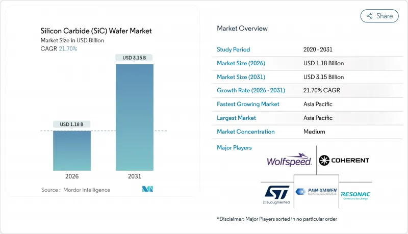
Silicon Carbide (SiC) Wafer - Market Share Analysis, Industry Trends & Statistics, Growth Forecasts (2026 - 2031)
The silicon carbide wafer market size in 2026 is estimated at USD 1.18 billion, growing from 2025 value of USD 0.97 billion with 2031 projections showing USD 3.15 billion, growing at 21.7% CAGR over 2026-2031.
The growth trajectory is supported by the automotive industry's migration to 800 V vehicle platforms, wide-band-gap adoption in industrial power electronics, and government incentives that underwrite new fabrication lines. Steadily improving crystal-growth yields, wider availability of 8-inch substrates, and rising demand for efficient fast-charging infrastructure further underpin expansion. Asia-Pacific held the largest regional share in 2024, and its vertically integrated ecosystem continues to attract upstream and downstream investments. Capital intensity remains a key competitive filter, yet companies that master defect reduction, wafer scaling, and internal supply chains are positioned to capture the next wave of demand as the silicon carbide wafer market outperforms conventional silicon in high-temperature and high-frequency operating environments.
Global Silicon Carbide (SiC) Wafer Market Trends and Insights
Rising EV Penetration and Shift Toward 800 V Vehicle Platforms
Automakers demonstrated large-scale 800 V system adoption through models such as Tesla's Model S Plaid, Hyundai's IONIQ 5, and Kia's EV6. These high-voltage architectures reduced charging times well below 20 minutes yet demanded power MOSFETs capable of withstanding elevated thermal and electrical stress. Silicon carbide meets these thresholds due to a ten-fold higher critical electric field and three-fold higher thermal conductivity than silicon, which magnifies demand in traction inverters and onboard chargers. Luxury and premium segments adopted the technology first, but falling wafer costs and maturing supply chains now accelerate diffusion into mainstream EV platforms, reinforcing the silicon carbide wafer market as an essential enabler of next-generation mobility.
Rapid Build-out of 800 V Charging Infrastructure
Charging network operators selected silicon carbide to minimise conversion losses in 350 kW stations. Electrify America's flagship sites integrated SiC-based rectifiers and DC-DC modules, achieving higher power density and lower heat dissipation compared with silicon. European corridor provider IONITY followed a similar path, creating a supply-demand flywheel that encourages automakers to embrace 800 V platforms. The resulting ecosystem, spanning vehicles, chargers, and grid-interfacing equipment, ramps up wafer volumes while compressing total ownership cost for network operators through energy-efficiency savings.
Limited Availability of 200 mm Substrates
Crystal-growth cycles for 200 mm boules often exceeded 200 hours and yielded higher defect densities than 150 mm equivalents, constraining the supply of automotive-grade substrates. Yield penalties elevated wafer ASPs and delayed design transitions to larger diameters. Fabricators invested in advanced in-situ monitoring and seed-crystal optimisation to close the gap, yet near-term shortages continue to cap silicon carbide wafer market shipment growth, especially for carmakers that require stringent quality thresholds.
Other drivers and restraints analyzed in the detailed report include:
- High-Temperature, High-Frequency Performance Advantages over Silicon
- Government Incentives for Wide-Band-Gap Fabs
- Packaging-Induced Thermo-Mechanical Stress
For complete list of drivers and restraints, kindly check the Table Of Contents.
Segment Analysis
The silicon carbide wafer market recorded 6-inch substrates at 53.75% share in 2025. Device counts per wafer and depreciation per die positioned this legacy diameter as the volume benchmark. However, 8-inch substrates are forecast to expand at a 28.6% CAGR through 2031, underscoring the cost-per-ampere advantage for traction inverters and PV inverters. Equipment investments remain high-PVT furnaces for 200 mm crystals cost USD 15-20 million versus USD 8-12 million for 6-inch. Nonetheless, each 8-inch wafer can deliver up to a 2.2-fold increase in die output, tightening the cost curve as yields improve. The silicon carbide wafer market size for 8-inch substrates is projected to command an increasingly large revenue pool as scale economies kick in.
Although yield rates lagged 6-inch equivalents by 15-20% in 2024, investment in hot-zone design optimisation and defect-reduction analytics narrowed the gap. Automotive and renewable energy integrators began qualification programs for 200 mm die, signalling broader acceptance once volume supply stabilises. less than 4-inch formats continued to decline as R&D moves toward high-voltage automotive or grid modules, while above 12-inch prototypes remained confined to academia. Successful scale-up to 8-inch thus stands as the pivotal inflection point for the silicon carbide wafer market.
N-type conductive wafers accounted for 68.12% of the silicon carbide wafer market share in 2025. Their low resistivity and stable dopant profiles made them indispensable for power MOSFETs, diodes, and Schottky devices. Semi-insulating substrates, although historically niche, are poised for 23.6% CAGR growth to 2031, driven by RF and microwave adoption in 5G base stations, radar, and satellite payloads. The silicon carbide wafer market size allocated to semi-insulating material is set to swell as network densification and defense electronics demand pure, electrically isolated lattices to limit parasitic capacitance at gigahertz frequencies.
Producers continue to refine post-growth annealing and compensation-doping techniques to lift resistivity uniformity across larger diameters. Aerospace and telecommunications firms favour semi-insulating wafers for GaN-on-SiC HEMTs that deliver superior thermal handling. As a result, the competitive landscape increasingly values substrates that ensure high thermal conductivity, electrical isolation, and superior RF performance. This trend highlights semi-insulating silicon carbide as a pivotal player in the evolution of next-generation device architectures.
Silicon Carbide (SiC) Wafer Market is Segmented by Wafer Diameter (less Than 4 Inch, and More), Conductivity Type (N-Type Conductive and Semi-Insulating), Application (Power Electronics, RF Devices, and More), End-Use Industry (Automotive and Electric Vehicles, Renewable Energy and Storage, and More), Crystal-Growth Technology (PVT, CVD, and More), and Geography. The Market Forecasts are Provided in Terms of Value (USD).
Geography Analysis
North America ranked second, bolstered by reshoring incentives and a deep EV ecosystem. Wolfspeed's Mohawk Valley fab ramped 200 mm wafers, and Tesla validated large-scale SiC traction inverters, spurring regional supply agreements. OnSemi committed up to USD 2 billion to establish end-to-end SiC production in the Czech Republic, providing optionality for European auto OEMs while retaining US technology leadership.chnology leadership through premium substrate production at ROHM and SK Siltron, preserving high ASPs despite down-price pressure.
North America ranked second, bolstered by reshoring incentives and a deep EV ecosystem. Wolfspeed's Mohawk Valley fab ramped 200 mm wafers, and Tesla validated large-scale SiC traction inverters, spurring regional supply agreements. OnSemi committed up to USD2 billion to establish end-to-end SiC production in the Czech Republic, providing optionality for European auto OEMs while retaining US technology leadership.
Europe advanced on the back of Green Deal electrification policies and a strong automotive base. Infineon expanded wafer output in Austria and Germany to serve Porsche and Audi 800 V platforms, emphasising quality and reliability over lowest cost. STMicroelectronics scaled its Catania site, anchoring a local supply chain that aligned with EU semiconductor sovereignty goals. Although the silicon carbide wafer market remained price sensitive, European buyers valued automotive-grade traceability and tight defect specifications.
- Wolfspeed Inc.
- Coherent Corp.
- Xiamen Powerway Advanced Material Co., Ltd.
- STMicroelectronics N.V.
- Resonac Holdings Corporation
- Atecom Technology Co., Ltd.
- SK Siltron Co., Ltd.
- SiCrystal GmbH
- Tankeblue Semiconductor Co., Ltd.
- Semiconductor Wafer Inc.
- GlobalWafers Co., Ltd.
- Sanan Optoelectronics Co., Ltd.
- ROHM Co., Ltd.
- Infineon Technologies AG
- onsemi Corporation
- Mitsubishi Electric Corporation
- Hebei Synlight Crystal Co., Ltd.
- Guangdong TySiC Semiconductor Co., Ltd.
- EpiWorld International Co., Ltd.
- Hench Semiconductor Co., Ltd.
- TYSTC Semiconductor Co., Ltd.
- ProChip Moissic Technologies Inc.
- Dow Silicon Carbide LLC
- Fraunhofer IISB (SiC Foundry)
- Nippon Steel & Sumitomo Metal SiC Materials Co., Ltd.
- LPE S.p.A.
Additional Benefits:
- The market estimate (ME) sheet in Excel format
- 3 months of analyst support
TABLE OF CONTENTS
1 INTRODUCTION
- 1.1 Study Assumptions and Market Definition
- 1.2 Scope of the Study
2 RESEARCH METHODOLOGY
3 EXECUTIVE SUMMARY
4 MARKET LANDSCAPE
- 4.1 Market Overview
- 4.2 Market Drivers
- 4.2.1 Rising EV penetration and shift toward 800-V vehicle platforms
- 4.2.2 Rapid build-out of 800 V charging infrastructure
- 4.2.3 High-temperature, high-frequency performance advantages over Si
- 4.2.4 Government incentives for wide-band-gap fabs
- 4.2.5 Emergence of vertically-integrated SiC supply chains in China
- 4.2.6 Novel 200 mm bulk-growth breakthroughs lowering defect density
- 4.3 Market Restraints
- 4.3.1 Limited availability of 200 mm substrates
- 4.3.2 Packaging-induced thermo-mechanical stress
- 4.3.3 Capital-intensive crystal-growth equipment
- 4.3.4 Recycling challenges for SiC kerf waste
- 4.4 Industry Value Chain Analysis
- 4.5 Regulatory Landscape
- 4.6 Technological Outlook
- 4.7 Impact of Macroeconomic Factors
- 4.8 Porter's Five Forces Analysis
- 4.8.1 Bargaining Power of Suppliers
- 4.8.2 Bargaining Power of Buyers
- 4.8.3 Threat of New Entrants
- 4.8.4 Threat of Substitutes
- 4.8.5 Intensity of Competitive Rivalry
5 MARKET SIZE AND GROWTH FORECASTS (VALUE)
- 5.1 By Wafer Diameter
- 5.1.1 less than 4 inch
- 5.1.2 6 inch
- 5.1.3 8 inch
- 5.1.4 above 12 inch
- 5.2 By Conductivity Type
- 5.2.1 N-Type Conductive
- 5.2.2 Semi-insulating
- 5.3 By Application
- 5.3.1 Power Electronics
- 5.3.2 Radio-Frequency Devices
- 5.3.3 Optoelectronics and LED
- 5.3.4 Other Applications
- 5.4 By End-use Industry
- 5.4.1 Automotive and Electric Vehicles
- 5.4.2 Renewable Energy and Storage
- 5.4.3 Telecommunications
- 5.4.4 Industrial Motor Drives and UPS
- 5.4.5 Aerospace and Defense
- 5.4.6 Other End-user Industries
- 5.5 By Crystal-Growth Technology
- 5.5.1 Physical Vapor Transport (PVT)
- 5.5.2 Chemical Vapor Deposition (CVD)
- 5.5.3 Modified Lely Sublimation
- 5.5.4 Other Technologies
- 5.6 By Geography
- 5.6.1 North America
- 5.6.1.1 United States
- 5.6.1.2 Canada
- 5.6.2 South America
- 5.6.2.1 Brazil
- 5.6.2.2 Argentina
- 5.6.2.3 Rest of South America
- 5.6.3 Europe
- 5.6.3.1 Germany
- 5.6.3.2 France
- 5.6.3.3 United Kingdom
- 5.6.3.4 Italy
- 5.6.3.5 Spain
- 5.6.3.6 Rest of Europe
- 5.6.4 Asia-Pacific
- 5.6.4.1 China
- 5.6.4.2 Japan
- 5.6.4.3 South Korea
- 5.6.4.4 Taiwan
- 5.6.4.5 India
- 5.6.4.6 Rest of Asia-Pacific
- 5.6.5 Middle East and Africa
- 5.6.5.1 Middle East
- 5.6.5.1.1 Saudi Arabia
- 5.6.5.1.2 United Arab Emirates
- 5.6.5.1.3 Rest of Middle East
- 5.6.5.2 Africa
- 5.6.5.2.1 South Africa
- 5.6.5.2.2 Nigeria
- 5.6.5.2.3 Rest of Africa
- 5.6.5.1 Middle East
- 5.6.1 North America
6 COMPETITIVE LANDSCAPE
- 6.1 Market Concentration
- 6.2 Strategic Moves
- 6.3 Market Share Analysis
- 6.4 Company Profiles (includes Global level Overview, Market level overview, Core Segments, Financials as available, Strategic Information, Market Rank/Share for key companies, Products and Services, and Recent Developments)
- 6.4.1 Wolfspeed Inc.
- 6.4.2 Coherent Corp.
- 6.4.3 Xiamen Powerway Advanced Material Co., Ltd.
- 6.4.4 STMicroelectronics N.V.
- 6.4.5 Resonac Holdings Corporation
- 6.4.6 Atecom Technology Co., Ltd.
- 6.4.7 SK Siltron Co., Ltd.
- 6.4.8 SiCrystal GmbH
- 6.4.9 Tankeblue Semiconductor Co., Ltd.
- 6.4.10 Semiconductor Wafer Inc.
- 6.4.11 GlobalWafers Co., Ltd.
- 6.4.12 Sanan Optoelectronics Co., Ltd.
- 6.4.13 ROHM Co., Ltd.
- 6.4.14 Infineon Technologies AG
- 6.4.15 onsemi Corporation
- 6.4.16 Mitsubishi Electric Corporation
- 6.4.17 Hebei Synlight Crystal Co., Ltd.
- 6.4.18 Guangdong TySiC Semiconductor Co., Ltd.
- 6.4.19 EpiWorld International Co., Ltd.
- 6.4.20 Hench Semiconductor Co., Ltd.
- 6.4.21 TYSTC Semiconductor Co., Ltd.
- 6.4.22 ProChip Moissic Technologies Inc.
- 6.4.23 Dow Silicon Carbide LLC
- 6.4.24 Fraunhofer IISB (SiC Foundry)
- 6.4.25 Nippon Steel & Sumitomo Metal SiC Materials Co., Ltd.
- 6.4.26 LPE S.p.A.
7 MARKET OPPORTUNITIES AND FUTURE OUTLOOK
- 7.1 White-space and Unmet-need Assessment

