
PUBLISHER: Mordor Intelligence | PRODUCT CODE: 1937414

PUBLISHER: Mordor Intelligence | PRODUCT CODE: 1937414
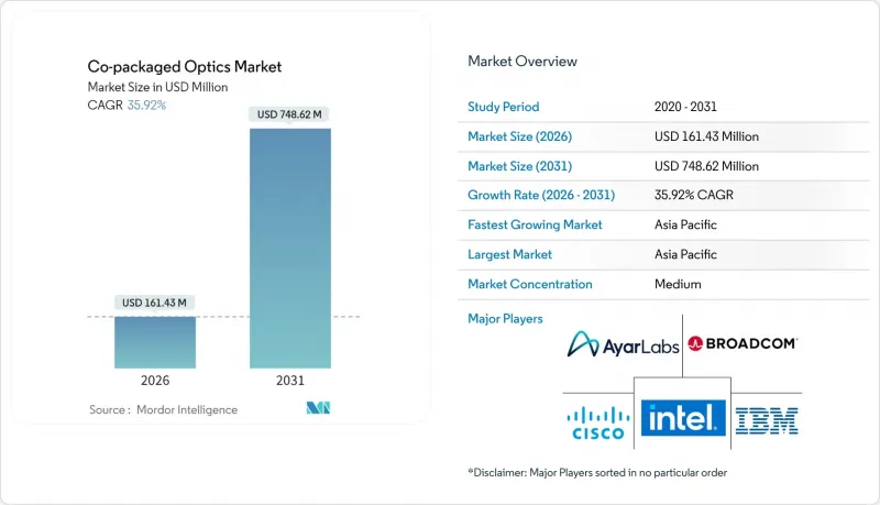
Co-packaged Optics - Market Share Analysis, Industry Trends & Statistics, Growth Forecasts (2026 - 2031)
The co-packaged optics market was valued at USD 0.12 billion in 2025 and estimated to grow from USD 0.16 billion in 2026 to reach USD 0.75 billion by 2031, at a CAGR of 35.92% during the forecast period (2026-2031).
Silicon photonics integration, once largely experimental, now benefits from high-volume semiconductor manufacturing and advanced packaging, enabling hyperscale operators to pursue bandwidth densities that match 51.2 Tbps switch silicon while lowering power budgets. Growth momentum stems from three reinforcing trends: (1) AI training clusters require far denser east-west bandwidth than classic cloud architectures, (2) energy-efficiency mandates in North America and the EU prioritize solutions that trim watt-per-gigabit metrics, and (3) foundry participation-most visibly TSMC's silicon-photonics packaging programs-reduces cost per optical lane and improves yield. Competitive intensity remains high as optical component vendors, semiconductor houses, and new silicon-photonics specialists race to solve heterogeneous-integration challenges that still constrain supply. As open compute communities refine interface specifications, the co-packaged optics market is positioned to shift from early adopter status to mainstream data-center infrastructure.
Global Co-packaged Optics Market Trends and Insights
Ramp-up of 51.2T switch silicon requiring 1.6T CPO
Broadcom's Bailly platform showed how embedding eight 6.4 Tbps optical engines beside a Tomahawk 5 switch delivered 70% lower power draw than pluggable transceivers. Hyperscale operators consequently reassessed network topologies because legacy electrical traces could not sustain the signal integrity demanded by 51.2 Tbps ASICs. The economic gap widened when rack-level thermal budgets for 800G pluggables hit practical ceilings, prompting procurement teams to treat co-packaged optics as a necessity rather than a lab project. As the third-generation CPO with 200 Gbit/s lanes enters production, the co-packaged optics market gains a clear technical roadmap that aligns with 2026-2028 switch-silicon refresh cycles. Equipment OEMs, therefore, accelerate design wins, locking in demand visibility over the medium term.
Hyperscale data-center energy-efficiency mandates
Net-zero pledges published by major cloud providers intensified scrutiny on watts-per-gigabit metrics. ASE's demonstration of <5 pJ/bit optical engines confirmed that integrating optics inside the switch package cuts DSP power and eliminates copper trace losses. Regulatory pressure-from carbon-pricing schemes in the EU to city-level moratoriums on new data-center builds-made the power reduction a board-level issue. Operators outlined three-year payback targets tied to energy savings and, in parallel, positioned co-packaged optics as a lever to unlock higher rack densities without breaching site power envelopes. The policy environment, therefore, transforms a technical benefit into an investment imperative, boosting demand through long-term purchase agreements.
Manufacturing complexity and heterogeneous integration yield
Co-packaged optics combines silicon photonics, III-V lasers, and advanced substrates inside a millimeter-scale envelope. Aligning optical waveguides to within tens of nanometers while also attaching high-power switch dice drives yields loss across multiple process steps. Recent yield slippages in advanced CoWoS lines, highlighted during NVIDIA's Blackwell ramp, underscore the fragile process window. Material-mismatch thermal stress necessitates exotic interface layers and active cooling, increasing part counts and inspection steps. Until learning curves mature, volume availability remains constrained, elongating lead times for tier-two OEMs and tempering near-term shipment forecasts for the co-packaged optics market.
Other drivers and restraints analyzed in the detailed report include:
- Surge in AI/ML cluster bandwidth demand
- Foundry participation enabling volume economics
- Interoperability and standards immaturity
For complete list of drivers and restraints, kindly check the Table Of Contents.
Segment Analysis
The 3.2 Tbps segment accounted for 37.92% of the co-packaged optics market revenue in 2025, reflecting the installed base of Tomahawk 4 class switches. However, >=6.4 Tbps devices are posting a 58.64% CAGR through 2031 as AI clusters press for higher radix fabrics. A single 6.4 Tbps engine co-located with a 51.2 Tbps ASIC yields eight optical lanes at 200 Gbit/s each, which halves the switch-to-module power budget and eliminates retimer stages. Vendors thus lock the >=6.4 Tbps roadmap into server refresh cycles beginning in 2026.
Looking forward, the foundry roadmaps project 12.8 Tbps engines that stack multiple optical cores within one package, positioning the top-end band to outgrow all other data-rate tiers. While sub-1.6 Tbps CPO remains viable for edge appliances where cost outranks density, hyperscale bidding documents now stipulate 200G/lane signal paths as a baseline. As this migration unfolds, the co-packaged optics market size for >=6.4 Tbps devices is set to outstrip the combined value of lower speed classes by 2029.
Optical engines represented 41.12% of 2025 revenue, yet laser sources are expanding at a 43.71% CAGR as vendors master on-chip light generation. China's integrated indium-phosphide laser arrays, produced on 200 mm silicon wafers, removed the need for external pump lasers and reduced package height, trimming material cost, and improved reliability.
Electronics ICs maintain steady demand as controller functions migrate on-package, but the incremental value pool is shifting toward laser innovation. With integrated sources eliminating fiber pigtails, system architects design slimmer top-of-rack switches and free front-panel real estate. The co-packaged optics market size for laser devices is therefore moving from niche to core, supported by multi-year supply agreements between hyperscalers and laser foundries.
Co-Packaged Optics Market is Segmented by Data Rate (< 1. 6T, 1. 6T, 3. 2T, and Above), Component (Optical Engine, Electrical IC, Laser Source, Connector and Packaging, and More), Integration Approach (On-Board Optics, and Co-Packaged Optics), End-Use Application (Hyperscale Cloud Data Centers, Enterprise Data Centers, and More), and Geography (North America, South America, Europe, Asia-Pacific, and Middle East and Africa).
Geography Analysis
Asia-Pacific commanded 32.78% of 2025 revenue and is advancing at a 41.99% CAGR, powered by government subsidies and vertically integrated supply. China's CNY 8.2 billion subsidy enabled eight-inch silicon-photonics wafer production and laser integration that compresses the bill-of-materials cost. Japan's Ministry of Economy, Trade and Industry funded USD 305 million for NTT, Intel, and SK Hynix to co-develop optical chips, strengthening local design ecosystems. South Korea complements the loop by aligning high-bandwidth memory roadmaps with optical interfaces.
North America supplies the bulk of end-user demand through hyperscale operators. Broadcom, Intel, and NVIDIA anchor the regional technology stack, while TSMC's Arizona fabs introduce domestic packaging capacity that shortens lead times for US cloud customers. The co-packaged optics market, therefore, benefits from a closed loop that links chip design to captive consumption, reinforcing the region's share even as production diversifies globally.
Europe prioritizes interoperability and sustainability. Open Compute Project chapters headquartered in the EU draft interface blueprints, shaping global deployment practices. Carbon-pricing legislation further propels adoption; operators document 30-50% power savings when shifting from pluggable optics to co-packaged lanes. M&A activity, typified by Nokia's USD 2.3 billion acquisition of Infinera, signals the region's intent to secure proprietary optical IP and climb the value chain.
- Ayar Labs Inc.
- Broadcom Inc.
- Cisco Systems Inc.
- IBM Corporation
- Intel Corporation
- Ranovus Inc.
- TE Connectivity Ltd.
- Furukawa Electric Co., Ltd.
- Hisense Broadband Multimedia Technology Co., Ltd.
- POET Technologies Inc.
- Kyocera Corporation
- HiSilicon (Huawei Technologies Co., Ltd.)
- SENKO Advanced Components, Inc.
- Sumitomo Electric Industries, Ltd.
- Coherent Corp.
- Taiwan Semiconductor Manufacturing Company Limited (TSMC)
- Lumentum Holdings Inc.
- NVIDIA Corporation
- Marvell Technology, Inc.
- Ciena Corporation
- Nokia Corporation
- InnoLight Technology (Suzhou) Ltd.
- Acacia Communications Inc.
- Hon Hai Precision Industry Co., Ltd. (Foxconn)
- Jabil Inc.
Additional Benefits:
- The market estimate (ME) sheet in Excel format
- 3 months of analyst support
TABLE OF CONTENTS
1 INTRODUCTION
- 1.1 Study Assumptions and Market Definition
- 1.2 Scope of the Study
2 RESEARCH METHODOLOGY
3 EXECUTIVE SUMMARY
4 MARKET LANDSCAPE
- 4.1 Market Overview
- 4.2 Market Drivers
- 4.2.1 Ramp-up of 51.2 T switch silicon requiring 1.6 T CPO
- 4.2.2 Hyperscale data-center energy-efficiency mandates
- 4.2.3 Surge in AI/ML cluster bandwidth demand
- 4.2.4 Transition to 800 G/1.6 T pluggables hitting thermal limits
- 4.2.5 Foundry participation (e.g., TSMC COUPE) enabling volume economics
- 4.2.6 Open Compute-driven CPO collaboration reducing vendor lock-in
- 4.3 Market Restraints
- 4.3.1 Manufacturing complexity and heterogeneous-integration yield
- 4.3.2 Interoperability and standards immaturity
- 4.3.3 Shift of optical-module ownership to switch-ASIC vendors
- 4.3.4 Photonic-packaging workforce skills gap
- 4.4 Value Chain Analysis
- 4.5 Regulatory Landscape
- 4.6 Technological Outlook
- 4.7 Impact of Macroeconomic Factors
- 4.8 Latency-Sensitive Traffic Impact
- 4.9 Porter's Five Forces Analysis
- 4.9.1 Threat of New Entrants
- 4.9.2 Bargaining Power of Buyers
- 4.9.3 Bargaining Power of Suppliers
- 4.9.4 Threat of Substitutes
- 4.9.5 Intensity of Competitive Rivalry
- 4.10 Investment and Funding Analysis
5 MARKET SIZE AND GROWTH FORECASTS (VALUE)
- 5.1 By Data Rate
- 5.1.1 < 1.6 T
- 5.1.2 1.6 T
- 5.1.3 3.2 T
- 5.1.4 6.4 T and Above
- 5.2 By Component
- 5.2.1 Optical Engine
- 5.2.2 Electrical IC
- 5.2.3 Laser Source
- 5.2.4 Connector and Packaging
- 5.2.5 Others
- 5.3 By Integration Approach
- 5.3.1 On-board Optics
- 5.3.2 Co-packaged Optics
- 5.4 By End-use Application
- 5.4.1 Hyperscale Cloud Data Centers
- 5.4.2 Enterprise Data Centers
- 5.4.3 Telco Central Offices
- 5.4.4 HPC and AI/ML Clusters
- 5.4.5 Others
- 5.5 By Geography
- 5.5.1 North America
- 5.5.1.1 United States
- 5.5.1.2 Canada
- 5.5.2 South America
- 5.5.2.1 Brazil
- 5.5.2.2 Rest of South America
- 5.5.3 Europe
- 5.5.3.1 Germany
- 5.5.3.2 United Kingdom
- 5.5.3.3 France
- 5.5.3.4 Netherlands
- 5.5.3.5 Rest of Europe
- 5.5.4 Asia-Pacific
- 5.5.4.1 China
- 5.5.4.2 Japan
- 5.5.4.3 South Korea
- 5.5.4.4 India
- 5.5.4.5 Rest of Asia-Pacific
- 5.5.5 Middle East and Africa
- 5.5.5.1 Middle East
- 5.5.5.1.1 Israel
- 5.5.5.1.2 Turkey
- 5.5.5.1.3 GCC
- 5.5.5.1.4 Rest of Middle East
- 5.5.5.2 Africa
- 5.5.5.2.1 South Africa
- 5.5.5.2.2 Rest of Africa
- 5.5.5.1 Middle East
- 5.5.1 North America
6 COMPETITIVE LANDSCAPE
- 6.1 Market Concentration
- 6.2 Strategic Moves
- 6.3 Market Share Analysis
- 6.4 Company Profiles (includes Global level Overview, Market level overview, Core Segments, Financials, Strategic Information, Market Rank/Share, Products and Services, Recent Developments)
- 6.4.1 Ayar Labs Inc.
- 6.4.2 Broadcom Inc.
- 6.4.3 Cisco Systems Inc.
- 6.4.4 IBM Corporation
- 6.4.5 Intel Corporation
- 6.4.6 Ranovus Inc.
- 6.4.7 TE Connectivity Ltd.
- 6.4.8 Furukawa Electric Co., Ltd.
- 6.4.9 Hisense Broadband Multimedia Technology Co., Ltd.
- 6.4.10 POET Technologies Inc.
- 6.4.11 Kyocera Corporation
- 6.4.12 HiSilicon (Huawei Technologies Co., Ltd.)
- 6.4.13 SENKO Advanced Components, Inc.
- 6.4.14 Sumitomo Electric Industries, Ltd.
- 6.4.15 Coherent Corp.
- 6.4.16 Taiwan Semiconductor Manufacturing Company Limited (TSMC)
- 6.4.17 Lumentum Holdings Inc.
- 6.4.18 NVIDIA Corporation
- 6.4.19 Marvell Technology, Inc.
- 6.4.20 Ciena Corporation
- 6.4.21 Nokia Corporation
- 6.4.22 InnoLight Technology (Suzhou) Ltd.
- 6.4.23 Acacia Communications Inc.
- 6.4.24 Hon Hai Precision Industry Co., Ltd. (Foxconn)
- 6.4.25 Jabil Inc.
7 MARKET OPPORTUNITIES AND FUTURE OUTLOOK
- 7.1 White-space and Unmet-need Assessment

