
PUBLISHER: Mordor Intelligence | PRODUCT CODE: 1940610

PUBLISHER: Mordor Intelligence | PRODUCT CODE: 1940610
Chemical Mechanical Planarization - Market Share Analysis, Industry Trends & Statistics, Growth Forecasts (2026 - 2031)
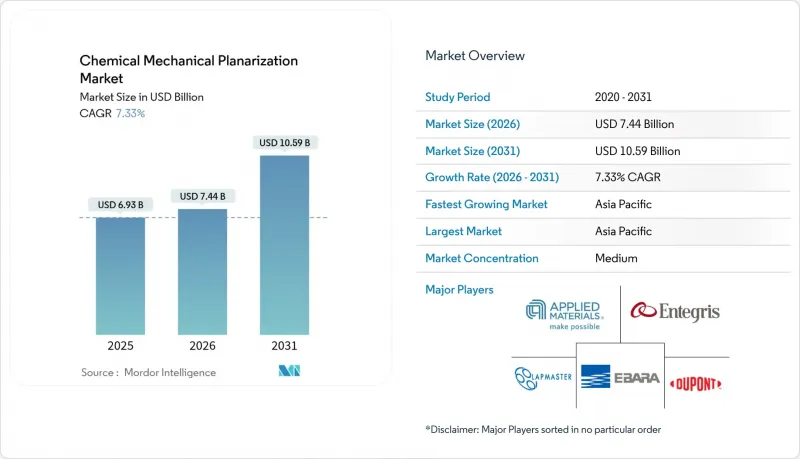
Chemical mechanical planarization market size in 2026 is estimated at USD 7.44 billion, growing from 2025 value of USD 6.93 billion with 2031 projections showing USD 10.59 billion, growing at 7.33% CAGR over 2026-2031.
Growth is propelled by the transition from FinFET to gate-all-around (GAA) transistors, 3D-integration, and the rising use of silicon carbide (SiC) and gallium nitride (GaN) in power devices. Foundries continue large-scale capacity additions, and government incentives in the United States and European Union encourage local CMP supply chains. Tight tool availability constrains production ramps, while sustainability initiatives accelerate demand for low-abrasive and abrasive-free slurries. Geopolitical export controls reshape equipment flows and spur parallel innovation tracks between Western and Chinese vendors.
Global Chemical Mechanical Planarization Market Trends and Insights
Accelerating GAA and 3D-IC adoption
Gate-all-around transistors alter CMP chemistries by introducing new metal gate stacks that require highly selective removal rates and tighter defectivity thresholds. Leading foundries have scheduled volume production of GAA nodes below 3 nm, driving an equipment refresh cycle for 300 mm single-wafer polishers with advanced endpoint control. Complementary 3D-integration techniques, such as through-silicon vias, demand ultra-flat copper layers across multiple wafer surfaces. CMP platforms, therefore, integrate closed-loop pad conditioning and real-time slurry monitoring to sustain yields at ever-smaller tolerances .
Rapid growth in SiC/GaN power devices
Silicon carbide and gallium nitride wafers exhibit hardness and chemical inertness that multiply polish times and consumable costs. Dedicated slurries using alkaline chemistries and engineered abrasives now achieve removal rates near 1 µm/h while holding surface roughness below 0.05 nm. Automotive electrification accelerates demand for these materials, prompting tool makers to release pad designs resilient to abrasive wear and cross-contamination shielding between SiC and traditional silicon lines.
Escalating slurry input costs
Cerium oxide, hydrogen peroxide, and other high-purity inputs show price spikes when rare-earth supply tightens or chemical plants undergo maintenance. The U.S. Geological Survey notes China remains the main source of rare-earth imports, leaving global slurry vendors exposed to trade disputes . Vendors respond by reformulating slurries with lower abrasive loads and recycling spent solutions through filtration loops.
Other drivers and restraints analyzed in the detailed report include:
- AI datacenter capital expenditure
- U.S. and EU fab incentives
- Tight OEM capacity for 300 mm tools
For complete list of drivers and restraints, kindly check the Table Of Contents.
Segment Analysis
Equipment represented 62.78% of the chemical mechanical planarization market size in 2025. Spending concentrates on single-wafer tools that deliver within-wafer non-uniformity below 1 nm and integrate closed-loop conditioning for pad surface health. The segment is forecast to rise at a 7.54% CAGR to 2031 as fabs install new platforms that support GAA processes and wide-bandgap substrates. Cleaning modules undergo concurrent upgrades to remove nanoscale defects at sub-7 nm nodes.
Consumables account for 37.22% of revenue, led by slurries whose recurring nature ensures stable demand. Silica-based dielectric slurries dominate, while niche ceria formulas address glass and sapphire polishing. Pad suppliers release grooved polymer blends that sustain consistent removal rates and minimize defectivity over extended pad life. Sustainability goals accelerate the shift to low-abrasive chemistries, positioning consumables vendors for premium pricing when performance and environmental metrics converge.
The Chemical Mechanical Planarization Market Report is Segmented by Product Type (CMP Equipment, CMP Consumables), Application (Integrated Circuit, Compound Semiconductor, MEMS and NEMS, Advanced Packaging, Other Applications), End-User (Foundries, Idms, OSAT, R&D Institutes/Universities), and Geography (North America, Europe, Asia Pacific, Rest of World). The Market Forecasts are Provided in Terms of Value (USD).
Geography Analysis
Asia Pacific generated 64.12% of 2025 revenue and is projected to record an 8.41% CAGR through 2031. Mainland China's localization push prompts aggressive wafer-fab construction, while Taiwan retains leadership in cutting-edge logic and advanced packaging. South Korea invests in high-layer count 3D NAND and DRAM, boosting demand for dielectric and metal planarization capacity. Japanese suppliers leverage decades-long expertise in ultrapure chemicals and precision pads, reinforcing the region's vertically integrated ecosystem.
North America ranks second by revenue. Federal incentives have unlocked new fab commitments, and domestic equipment leaders capture significant orders as customers prioritize secure supply chains. Advanced packaging initiatives in Arizona and New York stimulate regional demand for CMP consumables that comply with local content rules. Export controls limit high-end pad shipments to China, creating a bifurcated market and heightening strategic value for North American CMP vendors.
Europe pursues 20% global semiconductor output by 2030, emphasizing manufacturing sustainability. Regional materials firms expand electronics-grade hydrogen peroxide and specialty slurry capacity, while equipment makers in Germany and the Netherlands align CMP offerings with EU environmental directives. Government funding supports pilot lines for heterogeneous integration, driving incremental CMP tool installations across research hubs and specialty foundries.
- Applied Materials Inc.
- Entegris Inc.
- EBARA Corporation
- Lapmaster Wolters GmbH
- DuPont de Nemours, Inc.
- Fujimi Incorporated
- Revasum Inc.
- Resonac Holdings Corporation
- Okamoto Corporation
- FUJIFILM Corporation
- Tokyo Seimitsu Co., Ltd.
- Lam Research Corporation
- KLA Corporation
- Hitachi High-Tech Corporation
- Cabot Microelectronics Corporation
- 3M Company
- Saint-Gobain Surface Conditioning
- BASF SE
- Nagase ChemteX Corporation
- Ace Nanochem Co., Ltd.
Additional Benefits:
- The market estimate (ME) sheet in Excel format
- 3 months of analyst support
TABLE OF CONTENTS
1 INTRODUCTION
- 1.1 Study Assumptions and Market Definition
- 1.2 Scope of the Study
2 RESEARCH METHODOLOGY
3 EXECUTIVE SUMMARY
4 MARKET LANDSCAPE
- 4.1 Market Overview
- 4.2 Market Drivers
- 4.2.1 Accelerating GAA and 3D-IC adoption
- 4.2.2 Rapid growth in SiC/GaN power devices
- 4.2.3 Shrinking node-specific CMP step count
- 4.2.4 AI datacenter capex pull-through (advanced interconnect layers)
- 4.2.5 U.S. and EU fab incentives localizing CMP supply
- 4.2.6 Sustainability push for low-abrasive slurries
- 4.3 Market Restraints
- 4.3.1 Escalating slurry input costs (rare earths)
- 4.3.2 Tight OEM capacity for 300 mm tools
- 4.3.3 Cross-contamination risk in hetero-material CMP
- 4.3.4 China-US export controls on high-end pads and conditioners
- 4.4 Value / Supply-Chain Analysis
- 4.5 Regulatory Landscape
- 4.6 Technological Outlook
- 4.7 Porter Five Forces Analysis
- 4.7.1 Threat of New Entrants
- 4.7.2 Bargaining Power of Suppliers
- 4.7.3 Bargaining Power of Buyers
- 4.7.4 Threat of Substitutes
- 4.7.5 Competitive Rivalry
- 4.8 Investment Analysis
5 MARKET SIZE AND GROWTH FORECASTS (VALUE)
- 5.1 By Product Type
- 5.1.1 CMP Equipment
- 5.1.1.1 Single-Wafer CMP Systems
- 5.1.1.2 Post-CMP Cleaning Equipment
- 5.1.1.3 Batch CMP Systems
- 5.1.1.4 Others
- 5.1.2 CMP Consumables
- 5.1.2.1 CMP Slurry
- 5.1.2.1.1 Silica-Based Slurry
- 5.1.2.1.2 Aluminum Oxide-Based Slurry
- 5.1.2.1.3 Cerium Oxide-Based Slurry
- 5.1.2.1.4 Composite/Engineered Abrasive Slurry
- 5.1.2.1.5 Other (Zirconia, Diamond, etc.)
- 5.1.2.2 Pads
- 5.1.2.3 Other Consumables (Filters, Post-CMP Clean Chemistries, etc.)
- 5.1.2.1 CMP Slurry
- 5.1.1 CMP Equipment
- 5.2 By Application
- 5.2.1 Integrated Circuit
- 5.2.2 Compound Semiconductor
- 5.2.3 MEMS and NEMS
- 5.2.4 Advanced Packaging
- 5.2.5 Other Applications
- 5.3 By End-User
- 5.3.1 Foundries
- 5.3.2 Integrated Device Manufacturers (IDMs)
- 5.3.3 Outsourced Semiconductor Assembly and Test (OSAT)
- 5.3.4 R&D Institutes / Universities
- 5.4 By Geography
- 5.4.1 North America
- 5.4.1.1 United States
- 5.4.1.2 Canada
- 5.4.1.3 Mexico
- 5.4.2 Europe
- 5.4.2.1 Germany
- 5.4.2.2 France
- 5.4.2.3 United Kingdom
- 5.4.2.4 Italy
- 5.4.2.5 Rest of Europe
- 5.4.3 Asia Pacific
- 5.4.3.1 China
- 5.4.3.2 Japan
- 5.4.3.3 South Korea
- 5.4.3.4 India
- 5.4.3.5 Rest of Asia Pacific
- 5.4.4 South America
- 5.4.4.1 Brazil
- 5.4.4.2 Argentina
- 5.4.4.3 Rest of South America
- 5.4.5 Middle East
- 5.4.5.1 Israel
- 5.4.5.2 Saudi Arabia
- 5.4.5.3 United Arab Emirates
- 5.4.5.4 Rest of Middle East
- 5.4.6 Africa
- 5.4.6.1 South Africa
- 5.4.6.2 Egypt
- 5.4.6.3 Rest of Africa
- 5.4.1 North America
6 COMPETITIVE LANDSCAPE
- 6.1 Market Concentration Analysis
- 6.2 Strategic Moves and Developments
- 6.3 Vendor Positioning Analysis
- 6.4 Company Profiles (includes Global level Overview, Market level overview, Core Segments, Financials as available, Strategic Information, Products and Services, and Recent Developments)
- 6.4.1 Applied Materials Inc.
- 6.4.2 Entegris Inc.
- 6.4.3 EBARA Corporation
- 6.4.4 Lapmaster Wolters GmbH
- 6.4.5 DuPont de Nemours, Inc.
- 6.4.6 Fujimi Incorporated
- 6.4.7 Revasum Inc.
- 6.4.8 Resonac Holdings Corporation
- 6.4.9 Okamoto Corporation
- 6.4.10 FUJIFILM Corporation
- 6.4.11 Tokyo Seimitsu Co., Ltd.
- 6.4.12 Lam Research Corporation
- 6.4.13 KLA Corporation
- 6.4.14 Hitachi High-Tech Corporation
- 6.4.15 Cabot Microelectronics Corporation
- 6.4.16 3M Company
- 6.4.17 Saint-Gobain Surface Conditioning
- 6.4.18 BASF SE
- 6.4.19 Nagase ChemteX Corporation
- 6.4.20 Ace Nanochem Co., Ltd.
7 MARKET OPPORTUNITIES AND FUTURE OUTLOOK
- 7.1 White-space and Unmet-Need Assessment

