
PUBLISHER: Mordor Intelligence | PRODUCT CODE: 1940697

PUBLISHER: Mordor Intelligence | PRODUCT CODE: 1940697
Semiconductor Lithography Equipment - Market Share Analysis, Industry Trends & Statistics, Growth Forecasts (2026 - 2031)
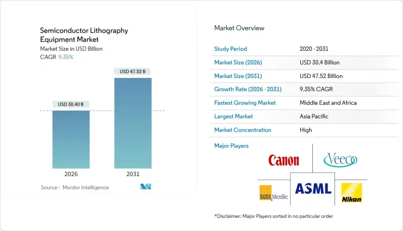
The semiconductor lithography equipment market is expected to grow from USD 27.8 billion in 2025 to USD 30.4 billion in 2026 and is forecast to reach USD 47.52 billion by 2031 at 9.35% CAGR over 2026-2031.
Momentum stems from the shift toward extreme ultraviolet (EUV) and forthcoming High-NA EUV platforms, the surge in artificial-intelligence servers, and multi-trillion-transistor graphics accelerators that demand denser patterning precision. Asia-Pacific remains the fulcrum of manufacturing capacity expansions, led by Taiwan's foundry dominance and South Korea's USD 471 billion mega-cluster program. Deep-ultraviolet (DUV) tools still anchor mature nodes, but the pipeline of High-NA EUV orders shows how quickly the ecosystem is pivoting toward sub-1 nm production. Capital-expenditure intensity and export-control compliance are the main brakes on diffusion, yet government subsidies, packaging innovations, and energy-efficient tool designs together widen the addressable base for advanced exposure systems.
Global Semiconductor Lithography Equipment Market Trends and Insights
Shrinking Process Nodes Drive EUV Adoption
Growing transistor density forces sub-7 nm geometries that only EUV can achieve. TSMC recorded first light on a High-NA tool in Hsinchu as it prepares 1 nm mass output by 2030. ASML's EXE platform reaches 8 nm resolution with anamorphic optics, a 40% imaging-contrast jump over prior NXE models. Research teams demonstrated 5 nm line-space interference printing, confirming far-below-roadmap capability. Server-class processors are projected to double to 200 billion transistors, magnifying lithography throughput needs. These milestones underline a rapid cadence toward angstrom dimensions that places High-NA tools at the center of capex priorities.
AI and Data-Center Demand for Leading-Edge Chips
Artificial-intelligence servers require multi-chiplet GPUs pushing past 2 trillion transistors. Semiconductor revenue is modeled to top USD 1 trillion by 2030, with AI accelerators and high-bandwidth memory as primary growth engines. Advanced packaging formats such as CoWoS intensify lithography overlay accuracy for redistribution layers. Samsung's heterogeneous-integration roadmap and TSMC's CoWoS capacity ramp have driven rush orders for large-panel exposure tools. Abu Dhabi's 1-5 GW AI compute cluster, featuring hundreds of thousands of GPUs, signals new geographies entering the capex cycle.
Ultra-High Capex of EUV Scanners
ASML's High-NA units list at USD 380 million each, double the cost of early EUV platforms. Total cost of ownership multiplies after clean-room reconfiguration, vibration isolation, and megawatt-class power-and-cooling utilities. Fewer than 20 High-NA machines are likely installed worldwide by end-2025, leaving mid-tier fabs locked out of the angstrom race. Research at the Okinawa Institute proposes a two-mirror projector and a 20-W source that could shrink power draw by 90%, hinting at future capex relief.
Other drivers and restraints analyzed in the detailed report include:
- Government Fab Subsidies Drive Equipment Investment
- Advanced-Packaging Boom Accelerates Equipment Demand
- Export-Control Restrictions to China
For complete list of drivers and restraints, kindly check the Table Of Contents.
Segment Analysis
In 2025, DUV platforms maintained 56.10% semiconductor lithography equipment market share, underlining their role in mature-node and cost-sensitive lines. High-NA EUV, although a smaller slice of the semiconductor lithography equipment market size today, is forecast to grow 10.54% CAGR through 2031 as single-exposure 1 nm imaging becomes a production reality. The 0.55 NA anamorphic projection inside ASML's EXE series improves depth-of-focus, enabling defect-density targets previously unattainable without quadruple patterning. Imec's 90% electrical yield on 20 nm pitch metal lines corroborates readiness for volume runs.
Conventional EUV remains indispensable for 5 nm logic, NAND flash, and DRAM refreshes, where 0.33 NA offers acceptable overlay with multi-patterning. Deep-UV immersion, already fully depreciated at many fabs, keeps the cost-per-die edge for analog, RF, and MEMS flows. Canon's nano-imprint pilot lines and Nikon's immersion enhancements signal niche competitive threats, yet ecosystem lock-in around ASML reticle formats sustains its platform moat.
The Semiconductor Lithography Machine Manufacturers Market is Segmented by Type (Deep Ultraviolet Lithography and Extreme Ultraviolet Lithography), Application (Advanced Packaging, MEMS Devices, and LED Devices), and Geography (North America, Europe, and More). The Market Forecasts are Provided in Terms of Value (USD).
Geography Analysis
Asia-Pacific's 67.60% share in 2025 reflects the agglomeration of logic and memory megafabs across Taiwan, South Korea, Japan, and mainland China. South Korea's USD 471 billion cluster will add multiple EUV suites, while Japan's government incentives lure TSMC into second-phase Kumamoto construction. China, despite export curbs, still spent USD 49 billion on overall fab tools in 2024 as domestic lithography projects scale.
North America ranks second, fueled by CHIPS Act co-funding that pushes combined Intel, TSMC, and Samsung U.S. projects past USD 200 billion. Arizona's twin-fab campus alone will deploy more than 25 EUV scanners over the forecast horizon. Fab clusters in Oregon, Ohio, and Texas broaden geographic redundancy and strengthen regional tool-service demand.
The Middle East and Africa, though small today, show a 12.48% CAGR. Saudi Arabia's SAR 1 billion venture fund underpins the National Semiconductor Hub, while UAE data-center projects necessitate local advanced-packaging capacity. Government-to-government technology-transfer accords expedite timeline compression, but workforce and supply-chain depth remain developmental bottlenecks.
- ASML Holding N.V.
- Nikon Corporation
- Canon Inc.
- Shanghai Micro Electronics Equipment (Group) Co., Ltd.
- SUSS MicroTec SE
- EV Group
- Veeco Instruments Inc.
- Onto Innovation Inc.
- JEOL Ltd.
- Neutronix Quintel Inc.
- Mycronic AB
- NuFlare Technology Inc.
- Ushio Inc.
- Ultratech (Veeco)
- Mapper Lithography B.V.
- Visitech AS
- KLA Corporation
- MKS Instruments (Newport)
- Inpria Corp.
- Tamarack Scientific Co.
Additional Benefits:
- The market estimate (ME) sheet in Excel format
- 3 months of analyst support
TABLE OF CONTENTS
1 INTRODUCTION
- 1.1 Study Assumptions and Market Definition
- 1.2 Scope of the Study
2 RESEARCH METHODOLOGY
3 EXECUTIVE SUMMARY
4 MARKET LANDSCAPE
- 4.1 Market Overview
- 4.2 Market Drivers
- 4.2.1 Shrinking process nodes drive EUV adoption
- 4.2.2 AI and data-center demand for leading-edge chips
- 4.2.3 Government fab subsidies (e.g., CHIPS Act)
- 4.2.4 Advanced-packaging boom (2.5D/3D IC)
- 4.2.5 High-NA EUV refresh accelerates tool cycles
- 4.2.6 Compound-semiconductor lithography demand
- 4.3 Market Restraints
- 4.3.1 Ultra-high capex of EUV scanners
- 4.3.2 Sub-system supply-chain bottlenecks
- 4.3.3 Sustainability and energy-use pressures
- 4.3.4 Export-control restrictions to China
- 4.4 Value Chain Analysis
- 4.5 Regulatory Landscape
- 4.6 Technological Outlook
- 4.7 Porter's Five Forces Analysis
- 4.7.1 Threat of New Entrants
- 4.7.2 Bargaining Power of Suppliers
- 4.7.3 Bargaining Power of Buyers
- 4.7.4 Threat of Substitutes
- 4.7.5 Competitive Rivalry
- 4.8 Pricing Analysis
- 4.9 Impact of Macroeconomic Factors
5 MARKET SIZE AND GROWTH FORECASTS (VALUE)
- 5.1 By Lithography Type
- 5.1.1 Deep Ultraviolet (DUV)
- 5.1.2 Extreme Ultraviolet (EUV)
- 5.1.3 High-NA EUV
- 5.2 By Application
- 5.2.1 Advanced Packaging
- 5.2.2 MEMS Devices
- 5.2.3 LED Devices
- 5.2.4 Power and Compound Semiconductors
- 5.3 By End-User
- 5.3.1 Pure-play Foundries
- 5.3.2 Integrated Device Manufacturers (IDMs)
- 5.3.3 Outsourced Semiconductor Assembly and Test (OSAT)
- 5.4 By Geography
- 5.4.1 North America
- 5.4.1.1 United States
- 5.4.1.2 Canada
- 5.4.1.3 Mexico
- 5.4.2 South America
- 5.4.2.1 Brazil
- 5.4.2.2 Argentina
- 5.4.2.3 Rest of South America
- 5.4.3 Europe
- 5.4.3.1 Germany
- 5.4.3.2 United Kingdom
- 5.4.3.3 France
- 5.4.3.4 Italy
- 5.4.3.5 Spain
- 5.4.3.6 Russia
- 5.4.3.7 Rest of Europe
- 5.4.4 Asia Pacific
- 5.4.4.1 China
- 5.4.4.2 Japan
- 5.4.4.3 India
- 5.4.4.4 South Korea
- 5.4.4.5 South East Asia
- 5.4.4.6 Rest of Asia Pacific
- 5.4.5 Middle East and Africa
- 5.4.5.1 Middle East
- 5.4.5.1.1 Saudi Arabia
- 5.4.5.1.2 United Arab Emirates
- 5.4.5.1.3 Turkey
- 5.4.5.1.4 Rest of Middle East
- 5.4.5.2 Africa
- 5.4.5.2.1 South Africa
- 5.4.5.2.2 Nigeria
- 5.4.5.2.3 Rest of Africa
- 5.4.5.1 Middle East
- 5.4.1 North America
6 COMPETITIVE LANDSCAPE
- 6.1 Market Concentration
- 6.2 Strategic Moves
- 6.3 Market Share Analysis
- 6.4 Company Profiles (includes Global level Overview, Market level overview, Core Segments, Financials as available, Strategic Information, Market Rank/Share for key companies, Products and Services, and Recent Developments)
- 6.4.1 ASML Holding N.V.
- 6.4.2 Nikon Corporation
- 6.4.3 Canon Inc.
- 6.4.4 Shanghai Micro Electronics Equipment (Group) Co., Ltd.
- 6.4.5 SUSS MicroTec SE
- 6.4.6 EV Group
- 6.4.7 Veeco Instruments Inc.
- 6.4.8 Onto Innovation Inc.
- 6.4.9 JEOL Ltd.
- 6.4.10 Neutronix Quintel Inc.
- 6.4.11 Mycronic AB
- 6.4.12 NuFlare Technology Inc.
- 6.4.13 Ushio Inc.
- 6.4.14 Ultratech (Veeco)
- 6.4.15 Mapper Lithography B.V.
- 6.4.16 Visitech AS
- 6.4.17 KLA Corporation
- 6.4.18 MKS Instruments (Newport)
- 6.4.19 Inpria Corp.
- 6.4.20 Tamarack Scientific Co.
7 MARKET OPPORTUNITIES AND FUTURE OUTLOOK
- 7.1 White-space and Unmet-Need Assessment

