
PUBLISHER: Mordor Intelligence | PRODUCT CODE: 2035027

PUBLISHER: Mordor Intelligence | PRODUCT CODE: 2035027
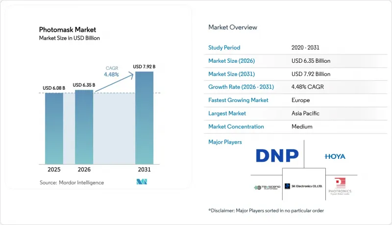
Photomask - Market Share Analysis, Industry Trends & Statistics, Growth Forecasts (2026 - 2031)
The photomask market size was valued at USD 6.08 billion in 2025 and estimated to grow from USD 6.35 billion in 2026 to reach USD 7.92 billion by 2031, at a CAGR of 4.48% during the forecast period (2026-2031).
Sustained demand for higher-resolution reticles, tighter critical-dimension control and defect-free mask blanks underpins this steady growth. Accelerated deployment of High-NA EUV tools in Taiwan and Korea is lifting average selling prices because every successive lithography node requires more sophisticated phase-shift engineering and absorber materials. The photomask market also benefits from the global push to localize semiconductor supply chains; new fabs in the United States and the European Union are choosing merchant mask outsourcing over in-house shops to optimize capital efficiency. Meanwhile, chiplet-based designs spur incremental demand for redistribution-layer (RDL) and interposer masks, spreading photomask consumption beyond front-end wafer processing into advanced packaging. Display panel makers moving to Gen 8+ AMOLED lines add another vector of growth because each new line consumes up to 30 unique display masks, elevating layer counts and revenue per fab.
Global Photomask Market Trends and Insights
High-NA EUV lithography adoption in Taiwan and Korea
Aggressive rollout of High-NA EUV tools marks the industry's transition into the angstrom era, forcing mask makers to deliver sub-10 nm pattern fidelity with near-zero printable defects. TSMC and Samsung now pay three to four times more per High-NA mask than for conventional EUV sets, expanding supplier revenue even as unit volumes stay stable. Korea's USD 471 billion semiconductor cluster plan includes captive photomask infrastructure, lowering import reliance and reshaping regional logistics. Tier-two foundries in China are expected to follow with delayed but inevitable adoption once export-control barriers ease. These developments collectively widen the technology gap between leading-edge and legacy photomask production, pushing legacy margins downward while boosting high-end profitability.
U.S./EU CHIPS Acts fueling merchant mask outsourcing
Domestic incentive programs worth USD 52.7 billion in the United States and comparable measures in Europe encourage new fabs that lack scale to build proprietary mask shops. Merchant suppliers are responding by colocating cleanrooms next to advanced fabs in Arizona, Ohio, and Dresden, improving cycle-times and geopolitical resilience. The regionalization thrust reduces over-dependence on Asia-Pacific sources, a strategic imperative amid rising tensions. Early outsourcing contracts stipulate dedicated toolsets for 3 nm and 2 nm nodes, locking in long-term revenue streams. Over time, merchant providers gain bargaining power as more single-site captive shops shutter to conserve capital.
EUV mask-blank defectivity above 5 defects/cm2 escalating scrap
Defect densities beyond the 5 defects/cm2 threshold force fabs to scrap up to 25% of EUV mask blanks, inflating costs by USD 50,000-100,000 each and delaying tape-out schedules. Limited qualified suppliers-mainly AGC and Shin-Etsu-struggle to scale volumes while meeting tighter specifications. Although new inspection optics and cleaning recipes lower particle counts, the road to sub-2 defects/cm2 remains uncertain. Persistent scrap erodes supplier margins and strains fab ramp-ups slated for 2025-2026. Any prolonged shortage could stall high-end mask deliveries and temper the photomask market CAGR.
Other drivers and restraints analyzed in the detailed report include:
- AMOLED Gen 8+ fabs driving 30-layer display masks
- Chiplet RDL and interposer photomasks upsurge
- Japan quartz-substrate supply bottlenecks
For complete list of drivers and restraints, kindly check the Table Of Contents.
Segment Analysis
Reticles generated the bulk of 2025 revenue, holding 65.90% of the photomask market, because every critical layer at sub-10 nm requires flawless image transfer to maintain line-edge roughness within spec. Premium pricing stems from the need to offset sophisticated resist interactions and phase-shift tuning. As High-NA EUV progresses, each device layer often demands bespoke illumination, expanding mask counts per wafer start. Master masks are growing fastest at a 4.99% CAGR because multi-patterning flows require high-fidelity templates that feed step-and-repeat daughter mask production. Copy and daughter masks still address legacy nodes but show subdued volume growth as advanced nodes take center stage. Collectively, the photomask market size for reticles and masters is expected to rise in tandem with wafer starts through 2031.
DNP's successful demonstration of EUV masks for beyond-2 nm processes underscores how product innovation secures competitive advantage. Reticle suppliers now integrate AI-based defect prediction to lower re-spin rates, improving fab cycle time. Volume manufacturing clusters in Taiwan and Korea favor vendors that can preload inventory near fabs for same-day deliveries, prompting investment in regional satellite sites. Given the high switching costs, customer loyalty remains strong once technical qualification is achieved, preserving revenue visibility across process generations.
Binary chrome masks held the largest 43.90% slice of the photomask market in 2025 thanks to cost-efficient manufacturing that continues to serve 65 nm and older nodes plus most display layers. Their enduring relevance anchors supplier cash flows during market lulls. EUV masks, however, carry the fastest 5.29% CAGR, fueled by sub-3 nm process ramps at foundries and IDMs. Each EUV mask sells at a multiple of optical chrome pricing, magnifying revenue despite lower unit volume. Attenuated and alternating phase-shift masks complement optical flows for critical layers, while nano-imprint templates establish a niche in memory patterning by offering high-throughput, low-cost alternatives when feature uniformity tolerates imprint variability.
The photomask market size for EUV products should expand as memory makers migrate select layers to EUV, adding density without new lithography options. Canon's nano-imprint roadmap keeps downward pressure on EUV pricing by signaling a substitute for specific applications, but EUV retains higher flexibility and throughput for diverse pattern geometries. Suppliers balance portfolios by keeping chrome capacity viable while funneling capital expenditures toward multibeam writers and pellicle lines required for EUV.
The Photomask Market Report is Segmented by Product Type (Reticle, Master Mask, and Copy/Daughter Mask), Mask Type (Binary Chrome Mask, Attenuated Phase Shift Mask, Alternating Phase Shift Mask, and More), Application (Semiconductor and IC Manufacturing, Flat-Panel Displays, and More), End-Use Industry (Foundries and IDMs, Fabless Design Houses, and More), and Geography. The Market Forecasts are Provided in Terms of Value (USD).
Geography Analysis
Asia-Pacific secured 71.10% of global sales in 2025 because Taiwan, Korea and China host the densest concentration of cutting-edge fabs and the most complete mask-making ecosystem. TSMC alone represents more than 60% of global foundry revenue, commanding massive reticle volumes each quarter. Complementary supply chains-quartz substrates from Shin-Etsu Chemical, multibeam writers from NuFlare and repair tools from Mycronic-enable same-region procurement, minimizing cycle-time risk. China continues adding mature-node capacity at a double-digit clip despite export constraints, ensuring ongoing demand for optical chrome masks. Korea's USD 471 billion cluster plan adds 16 new fabs through 2047, each with dedicated photomask infrastructure, reinforcing Asia-Pacific pre-eminence.
Europe is growing fastest at 4.55% CAGR as governments fund semiconductor sovereignty programs under the European Chips Act. Tekscend Photomask's multibeam installation in Dresden cuts writing time for complex masks from days to mere hours, signaling continental readiness for advanced-node production. Germany anchors the region through ZEISS SMT's expansion of mask-solutions sites in Jena, Oberkochen and Wetzlar, aligning optics, blanks and writing to local fab needs. Strategic focus rests on automotive and industrial chips, where Europe already wields design and systems expertise, augmenting domestic photomask uptake.
North America benefits from USD 52.7 billion in CHIPS Act incentives that spur fab projects in Arizona, Ohio and New York, creating fresh demand for proximate mask suppliers. TSMC's USD 165 billion Arizona complex alone will consume thousands of EUV masks annually, inviting both Asian and European vendors to establish local satellite operations. Intel's foundry push, GlobalFoundries' expansions and multiple specialty fabs together diversify the customer base. However, cost structures remain higher than in Asia-Pacific, so profit margins depend on value-added services such as rapid-turn prototypes and on-site defect analysis.
- Tekscend Photomask Inc. (Toppan)
- Dai Nippon Printing Co., Ltd.
- Photronics, Inc.
- Hoya Corporation
- SK-Electronics Co., Ltd.
- Nippon Filcon Co., Ltd.
- Compugraphics International Ltd.
- Taiwan Mask Corporation
- Mycronic AB
- LG Innotek Co., Ltd.
- Advanced Mask Technology Center GmbH
- Shenzhen Qingyi Photomask Ltd.
- NuFlare Technology Inc.
- Canon Inc.
- IMS Nanofabrication GmbH
- Applied Materials, Inc.
- ASML Holding N.V.
- Fujifilm Holdings Corp.
- Advantest Corp.
- Vistec Electron Beam
- JENOPTIK AG
Additional Benefits:
- The market estimate (ME) sheet in Excel format
- 3 months of analyst support
TABLE OF CONTENTS
1 INTRODUCTION
- 1.1 Study Assumptions and Market Definition
- 1.2 Scope of the Study
2 RESEARCH METHODOLOGY
3 EXECUTIVE SUMMARY
4 MARKET LANDSCAPE
- 4.1 Market Overview
- 4.2 Market Drivers
- 4.2.1 High-NA EUV Lithography Adoption in Taiwan and Korea
- 4.2.2 U.S./EU CHIPS Acts Fueling Merchant Mask Outsourcing
- 4.2.3 AMOLED Gen 8+ Fabs Driving 30-Layer Display Masks
- 4.2.4 ADAS and Power-SemiLess than 28 nm Demand for Large-Area Reticles
- 4.2.5 Chiplet RDL and Interposer Photomasks Upsurge
- 4.2.6 AI-Enabled Defect Inspection Cutting TAT for Captive Shops
- 4.3 Market Restraints
- 4.3.1 EUV Mask-Blank Defectivity Above 5 defects/cm2 Escalating Scrap
- 4.3.2 Japan Quartz-Substrate Supply Bottlenecks
- 4.3.3 Export Controls on Multi-Beam Writers Limiting China
- 4.3.4 Rising Electricity Tariffs in Korea and Taiwan
- 4.4 Industry Ecosystem Analysis
- 4.5 Technological Outlook
- 4.6 Porter's Five Forces Analysis
- 4.6.1 Bargaining Power of Suppliers
- 4.6.2 Bargaining Power of Buyers
- 4.6.3 Threat of New Entrants
- 4.6.4 Threat of Substitutes
- 4.6.5 Competitive Rivalry
5 MARKET SIZE AND GROWTH FORECASTS (VALUES)
- 5.1 By Product Type
- 5.1.1 Reticle (4X/5X)
- 5.1.2 Master Mask
- 5.1.3 Copy/Daughter Mask
- 5.2 By Mask Type
- 5.2.1 Binary Chrome Mask (BCM)
- 5.2.2 Attenuated Phase Shift Mask (Att-PSM)
- 5.2.3 Alternating Phase Shift Mask (Alt-PSM)
- 5.2.4 Chromeless Phase Lithography Mask
- 5.2.5 EUV Photomask
- 5.2.6 Nano-imprint Template
- 5.3 By Application
- 5.3.1 Semiconductor and IC Manufacturing
- 5.3.1.1 More than 65 nm
- 5.3.1.2 45-28 nm
- 5.3.1.3 22-14 nm
- 5.3.1.4 10-7 nm
- 5.3.1.5 5 nm
- 5.3.1.6 Upto 3 nm
- 5.3.2 Flat-Panel Displays
- 5.3.2.1 LCD
- 5.3.2.2 AMOLED
- 5.3.2.3 OLED Micro-display
- 5.3.3 MEMS Sensors
- 5.3.4 Advanced Packaging (RDL/Interposer)
- 5.3.5 Photonics and Silicon Photonics
- 5.3.6 Others
- 5.3.1 Semiconductor and IC Manufacturing
- 5.4 By End-use Industry
- 5.4.1 Foundries and IDMs
- 5.4.2 Fabless Design Houses
- 5.4.3 Display Panel Manufacturers
- 5.4.4 OSAT/Advanced Packaging Providers
- 5.4.5 Research and Academia
- 5.4.6 Aerospace and Defense
- 5.4.7 Telecommunications OEMs
- 5.5 By Geography
- 5.5.1 North America
- 5.5.1.1 United States
- 5.5.1.2 Canada
- 5.5.1.3 Mexico
- 5.5.2 Europe
- 5.5.2.1 Germany
- 5.5.2.2 United Kingdom
- 5.5.2.3 France
- 5.5.2.4 Nordics
- 5.5.2.5 Rest of Europe
- 5.5.3 South America
- 5.5.3.1 Brazil
- 5.5.3.2 Rest of South America
- 5.5.4 Asia-Pacific
- 5.5.4.1 China
- 5.5.4.2 Japan
- 5.5.4.3 India
- 5.5.4.4 South-East Asia
- 5.5.4.5 Rest of Asia-Pacific
- 5.5.5 Middle East and Africa
- 5.5.5.1 Middle East
- 5.5.5.1.1 Gulf Cooperation Council Countries
- 5.5.5.1.2 Turkey
- 5.5.5.1.3 Rest of Middle East
- 5.5.5.2 Africa
- 5.5.5.2.1 South Africa
- 5.5.5.2.2 Rest of Africa
- 5.5.5.1 Middle East
- 5.5.1 North America
6 COMPETITIVE LANDSCAPE
- 6.1 Market Concentration
- 6.2 Strategic Moves
- 6.3 Market Share Analysis
- 6.4 Company Profiles {(includes Global level Overview, Market level overview, Core Segments, Financials as available, Strategic Information, Market Rank/Share for key companies, Products and Services, and Recent Developments)}
- 6.4.1 Tekscend Photomask Inc. (Toppan)
- 6.4.2 Dai Nippon Printing Co., Ltd.
- 6.4.3 Photronics, Inc.
- 6.4.4 Hoya Corporation
- 6.4.5 SK-Electronics Co., Ltd.
- 6.4.6 Nippon Filcon Co., Ltd.
- 6.4.7 Compugraphics International Ltd.
- 6.4.8 Taiwan Mask Corporation
- 6.4.9 Mycronic AB
- 6.4.10 LG Innotek Co., Ltd.
- 6.4.11 Advanced Mask Technology Center GmbH
- 6.4.12 Shenzhen Qingyi Photomask Ltd.
- 6.4.13 NuFlare Technology Inc.
- 6.4.14 Canon Inc.
- 6.4.15 IMS Nanofabrication GmbH
- 6.4.16 Applied Materials, Inc.
- 6.4.17 ASML Holding N.V.
- 6.4.18 Fujifilm Holdings Corp.
- 6.4.19 Advantest Corp.
- 6.4.20 Vistec Electron Beam
- 6.4.21 JENOPTIK AG
7 MARKET OPPORTUNITIES AND FUTURE OUTLOOK
- 7.1 White-space and Unmet-Need Assessment

