
PUBLISHER: Mordor Intelligence | PRODUCT CODE: 2035033

PUBLISHER: Mordor Intelligence | PRODUCT CODE: 2035033
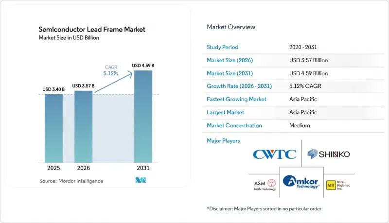
Semiconductor Lead Frame - Market Share Analysis, Industry Trends & Statistics, Growth Forecasts (2026 - 2031)
The semiconductor lead frame market size was valued at USD 3.40 billion in 2025 and estimated to grow from USD 3.57 billion in 2026 to reach USD 4.59 billion by 2031, at a CAGR of 5.12% during the forecast period (2026-2031).
Demand accelerated as automotive electronics, 5G infrastructure, and AI-enabled edge devices required compact packages that dissipate heat effectively while supporting high-speed signals. Miniaturization shifted unit volumes toward Quad Flat No-Lead (QFN) and Dual Flat No-Lead (DFN) variants, and power-electronics adoption in electric vehicles (EVs) lifted specifications for copper-based frames able to endure higher thermal loads. Regionalization of supply chains gathered momentum as the CHIPS Act prompted fresh capacity in North America and Europe, complementing entrenched production hubs in Asia-Pacific. At the same time, composite and multi-layer structures gained traction as material innovations aimed to counter copper and silver price volatility and support silicon carbide (SiC) and gallium nitride (GaN) technologies.
Global Semiconductor Lead Frame Market Trends and Insights
Consumer-electronics demand spike
Surging smartphone, wearable, and gaming-device shipments in 2024 and early 2025 tightened product-development cycles and pushed designers toward slimmer QFN outlines that improved thermal paths without enlarging footprints. Roughly one quarter of global output already uses lead-frame thicknesses below 0.1 mm, enabling higher component density inside premium mobiles. Several OSAT providers extended automotive-qualified flows to consumer lines, promoting Grade-0 reliability in handheld products that faced frequent temperature swings. These shifts sustained the semiconductor lead frame market as device makers balanced battery life, weight, and performance requirements.
EV and xEV power-electronics boom
Electric-vehicle production climbed sharply, and traction inverters shifted from 400 V to 800 V architectures. Lead frames, therefore, require copper alloys with improved thermal conductivity and fatigue strength. ROHM's TRCDRIVE pack(TM) SiC module illustrated the need for optimized heat spreading to maintain low switching losses up to 300 kW. Tier-1 suppliers specified composite frames that paired stamped copper with plated nickel-palladium finishes to control corrosion over extended vehicle lifetimes. The automotive procurement wave broadened revenue visibility and anchored long-term orders within the semiconductor lead frame market.
CAPEX intensity and production bottlenecks
Turnkey stamping lines with fine-pitch capability exceeded USD 300 million per site, and tooling costs rose as die pads shrank. Smaller vendors faced liquidity strains, pushing some to merge or license capacity from larger OSATs. High automation levels, including AI-enabled defect-inspection networks with 95% accuracy, partially offset labour shortages but lengthened ramp timelines. Capacity tightness occasionally delays customer qualifications, creating a headwind for the semiconductor lead frame market.
Other drivers and restraints analyzed in the detailed report include:
- 5G/AI edge devices needing QFN/QFP
- Asia-Pacific capacity additions
- Copper and Ag price volatility
For complete list of drivers and restraints, kindly check the Table Of Contents.
Segment Analysis
QFN packages captured 31.65% of 2025 volumes, confirming their role as the preferred choice for thermal efficiency in limited board area. The segment's evolution toward smaller lead pitches and center pads bolstered reliability in automotive sensors and premium smartphones. DFN units, projected to deliver an 8.45% CAGR to 2031, offered even thinner profiles suited to wearables and compact IoT end-nodes. Together, QFN and DFN sustained healthy revenue streams that kept the semiconductor lead frame market on its upward trajectory.
Advances such as drop-in heat slugs and double-die stacking expanded QFP use cases, while DIP and SOP packages gradually migrated to legacy or industrial markets where cost outweighed miniaturization. Flip-chip outlines served high-performance computing but required plated copper pillars rather than exposed leads. Across the category, the semiconductor lead frame market size for QFN and DFN was forecast to outpace wider industry growth, driven by continuous smartphone refresh cycles and regulatory pushes for lighter in-car modules.
Stamping maintained 62.75% of 2025 production thanks to high-speed presses exceeding 90,000 strokes per hour and modular die sets that reduced changeover time. Continuous strip plating added selective finishes that limited precious-metal usage. Multi-layer composites, however, are expected to register a 9.05% CAGR through 2031 as designers combine copper cores with inlaid molybdenum or aluminium for thermal spreading. These premium configurations reflect the semiconductor lead frame market's response to EV inverter stress conditions.
Etching found a share in small-lot, high-precision circuits for 5G beamformers and optical modules. Laser-assisted photoresist exposure improved edge acuity, allowing +-5 µm dimensional control. As complexity rose, the semiconductor lead frame industry allocated research and development toward hybrid flows that used etching for fine features and stamping for mechanical robustness, balancing cost and performance under tightened product-launch windows.
Semiconductor Lead Frame Market is Segmented by Packaging Type (DIP (Dual In-Line Package), SOP (Small Outline Package), and More), Manufacturing Process (Stamping Lead Frame, Etching Lead Frame, and More), Application (Integrated Circuits, Discrete Devices, and More), Industry Vertical (Consumer Electronics, Automotive, and More), and Geography (North America, South America, Europe, Asia-Pacific, and Middle East and Africa).
Geography Analysis
Asia-Pacific held 41.10% of global revenue in 2025 and was expected to log a 8.75% CAGR through 2031. China shipped more than 42 billion stamped frames, while Japan's precision-etch specialists supplied high-frequency modules for driver-assistance systems. Investments exceeding USD 300 million in Vietnam and Malaysia upgraded plating lines to support SiC power hybrids.
North America saw renewed impetus from the CHIPS Act, which earmarked USD 39 billion for fabrication expansion and USD 13.2 billion for R&D. Fab capacity was projected to rise 203% by 2032, creating demand for domestically sourced frames that matched heterogeneous-integration roadmaps. Intel's EMIB and Foveros programs required custom copper-alloy compositions, adding value layers that differentiated suppliers.
Europe concentrated on high-reliability automotive and industrial uses, supported by the Euro 43 billion (USD 49.90 billion) European Chips Act, aiming for 20% global semiconductor output by 2030. Limited local IC-substrate capability left white-space for new entrants ready to establish composite or etched-frame lines near Germany's car manufacturers. Raw-material price escalation-copper up 9% and aluminium up 8%-drove European firms to explore recycling initiatives that aligned with carbon-reduction mandates, reinforcing supply-chain resilience in the semiconductor lead frame industry.
- Mitsubishi Materials Corporation
- Amkor Technology Inc.
- SHINKO ELECTRIC INDUSTRIES CO., LTD.
- Precision Micro Ltd.
- Maxell, Ltd.
- ROHM MECHATECH
- Technic Inc.
- SDI Group, Inc.
- Dai Nippon Printing Co., Ltd.
- Sun Industry Co., Ltd.
- ECE
- Mitsui High-tec, Inc.
- ASM Pacific Technology Ltd.
- Chang Wah Technology Co., Ltd.
- Resonac Corporation
- Jentech Precision Industrial
- Nippon Micro Metal Corp.
- Hitek Fine Metal Co., Ltd.
- SDI Malaysia
- Possehl Electronics
- Jiangsu Hengxin Technology
- Haesung DS Co., Ltd.
- Carsem (M) Sdn Bhd
- Ningbo Kangqiang
Additional Benefits:
- The market estimate (ME) sheet in Excel format
- 3 months of analyst support
TABLE OF CONTENTS
1 INTRODUCTION
- 1.1 Study Assumptions and Market Definition
- 1.2 Scope of the Study
2 RESEARCH METHODOLOGY
3 EXECUTIVE SUMMARY
4 MARKET LANDSCAPE
- 4.1 Market Overview
- 4.2 Market Drivers
- 4.2.1 Consumer-electronics demand spike
- 4.2.2 EV and xEV power-electronics boom
- 4.2.3 5G/AI edge devices needing QFN/QFP
- 4.2.4 Asia-Pacific capacity additions
- 4.2.5 SiC/GaN modules favour Cu lead frames
- 4.2.6 CHIPS-Act-driven on-shore packaging CAPEX
- 4.3 Market Restraints
- 4.3.1 CAPEX intensity and production bottlenecks
- 4.3.2 Copper and Ag price volatility
- 4.3.3 Shift to glass/organic interposers
- 4.3.4 Stricter plating-chemical regulations
- 4.4 Value Chain Analysis
- 4.5 Regulatory Landscape
- 4.6 Technological Outlook
- 4.7 Porter's Five Forces Analysis
- 4.7.1 Threat of New Entrants
- 4.7.2 Bargaining Power of Buyers
- 4.7.3 Bargaining Power of Suppliers
- 4.7.4 Threat of Substitutes
- 4.7.5 Intensity of Competitive Rivalry
- 4.8 Investment Landscape (CAPEX and M&A)
- 4.9 Impact on Macroeconomic factors
5 MARKET SIZE AND GROWTH FORECASTS (VALUE)
- 5.1 By Packaging Type
- 5.1.1 DIP (Dual In-Line Package)
- 5.1.2 SOP (Small Outline Package)
- 5.1.3 SOT (Small Outline Transistor)
- 5.1.4 QFP (Quad Flat Pack)
- 5.1.5 DFN (Dual Flat No-Lead)
- 5.1.6 QFN (Quad Flat No-Lead)
- 5.1.7 FC and TO Packages
- 5.2 By Manufacturing Process
- 5.2.1 Stamping Lead Frame
- 5.2.2 Etching Lead Frame
- 5.2.3 Multi-layer / Composite
- 5.3 By Application
- 5.3.1 Integrated Circuits
- 5.3.2 Discrete Devices
- 5.3.3 Power Modules
- 5.3.4 MEMS and Sensors
- 5.4 By Industry Vertical
- 5.4.1 Consumer Electronics
- 5.4.2 Automotive
- 5.4.3 Industrial and Commercial Electronics
- 5.4.4 Telecommunications
- 5.4.5 Aerospace and Defence
- 5.4.6 Medical Devices
- 5.5 By Geography
- 5.5.1 North America
- 5.5.1.1 United States
- 5.5.1.2 Canada
- 5.5.2 South America
- 5.5.2.1 Brazil
- 5.5.2.2 Argentina
- 5.5.2.3 Rest of South America
- 5.5.3 Europe
- 5.5.3.1 Germany
- 5.5.3.2 United Kingdom
- 5.5.3.3 France
- 5.5.3.4 Italy
- 5.5.3.5 Russia
- 5.5.3.6 Rest of Europe
- 5.5.4 Asia-Pacific
- 5.5.4.1 China
- 5.5.4.2 Japan
- 5.5.4.3 South Korea
- 5.5.4.4 India
- 5.5.4.5 ASEAN
- 5.5.4.6 Rest of Asia-Pacific
- 5.5.5 Middle East and Africa
- 5.5.5.1 Middle East
- 5.5.5.1.1 GCC
- 5.5.5.1.2 Rest of Middle East
- 5.5.5.2 Africa
- 5.5.5.2.1 South Africa
- 5.5.5.2.2 Rest of Africa
- 5.5.5.1 Middle East
- 5.5.1 North America
6 COMPETITIVE LANDSCAPE
- 6.1 Market Concentration
- 6.2 Strategic Moves
- 6.3 Market Share Analysis
- 6.4 Company Profiles (includes Global level Overview, Market level overview, Core Segments, Financials as available, Strategic Information, Market Rank/Share, Products and Services, Recent Developments)
- 6.4.1 Mitsubishi Materials Corporation
- 6.4.2 Amkor Technology Inc.
- 6.4.3 SHINKO ELECTRIC INDUSTRIES CO., LTD.
- 6.4.4 Precision Micro Ltd.
- 6.4.5 Maxell, Ltd.
- 6.4.6 ROHM MECHATECH
- 6.4.7 Technic Inc.
- 6.4.8 SDI Group, Inc.
- 6.4.9 Dai Nippon Printing Co., Ltd.
- 6.4.10 Sun Industry Co., Ltd.
- 6.4.11 ECE
- 6.4.12 Mitsui High-tec, Inc.
- 6.4.13 ASM Pacific Technology Ltd.
- 6.4.14 Chang Wah Technology Co., Ltd.
- 6.4.15 Resonac Corporation
- 6.4.16 Jentech Precision Industrial
- 6.4.17 Nippon Micro Metal Corp.
- 6.4.18 Hitek Fine Metal Co., Ltd.
- 6.4.19 SDI Malaysia
- 6.4.20 Possehl Electronics
- 6.4.21 Jiangsu Hengxin Technology
- 6.4.22 Haesung DS Co., Ltd.
- 6.4.23 Carsem (M) Sdn Bhd
- 6.4.24 Ningbo Kangqiang
7 MARKET OPPORTUNITIES AND FUTURE OUTLOOK
- 7.1 White-space and Unmet-need Assessment

