
PUBLISHER: Mordor Intelligence | PRODUCT CODE: 2035097

PUBLISHER: Mordor Intelligence | PRODUCT CODE: 2035097
Panel Level Packaging - Market Share Analysis, Industry Trends & Statistics, Growth Forecasts (2026 - 2031)
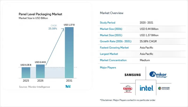
The panel-level packaging market size is expected to grow from USD 0.35 billion in 2025 to USD 0.44 billion in 2026 and is forecast to reach USD 1.37 billion by 2031 at 25.58% CAGR over 2026-2031.
The steep trajectory mirrors the semiconductor sector's shift from wafer-centric to panel-centric architectures, a move that unlocks scale advantages and aligns with burgeoning AI and high-performance computing demand. Panel formats deliver up to 40% better substrate utilization for multi-die designs, easing cost pressure as logic and memory nodes scale below 5 nm. Substrate innovation, notably the transition toward glass cores, promises tighter dimensional control and improved thermal stability, which together support rising input/output counts. Equipment vendors have responded with 600 mm X 600 mm lithography systems capable of sub-10 µm features, erasing a former resolution ceiling and widening the addressable market for next-generation integration. Supply-chain coordination is intensifying, illustrated by vertically integrated strategies from leading foundries and by cooperative capacity expansions between foundry and OSAT partners.
Global Panel Level Packaging Market Trends and Insights
Cost Reduction Versus Wafer-Level Packaging
Moving to panel formats yields up to 40% better substrate utilization for multi-die designs, cutting cost per placement even after accounting for expensive tooling. ASE's USD 200 million investment in 310 mm X 310 mm lines signals a commitment to volume scaling, and high-volume consumer devices supply the wafer starts needed to amortize tools across short life cycles. Asian contract manufacturers gain further leverage by clustering substrate fabrication, redistribution-layer processing, and final test inside single campuses, reducing logistics overhead. Western houses with lower volumes face a steeper cost curve, widening the competitiveness gap. As a result, panel-first strategies increasingly determine win rates in turnkey package bids.
Surge of AI/HPC Chip Demand
Large language-model inference and training floors require ever-denser GPU clusters, driving packaging toward larger interposer-free footprints that sustain bandwidth. TSMC's Chip-on-Panel-on-Substrate (CoPoS) roadmap, slated for 2027 risk production, doubles reticle-limited dimensions of CoWoS while holding thermal resistance steady. The foundry is expanding CoWoS capacity more than 60% annually through 2026, yet still projects backlog in high-bandwidth memory (HBM) lines, pushing Tier-1 customers to evaluate panel-level packaging market alternatives for next-generation accelerator cards. Early movers able to demonstrate >20 kW shelf-level cooling in panel packages are best positioned to secure multi-year supply agreements.
High Capital Intensity and Warpage Issues
A full 600 mm line demands more than USD 500 million in deposition, patterning, and metrology gear. Panel substrates expand under thermal load, generating a bow that can exceed 2 mm if not compensated. SK Key Foundry and LB Semicon's Direct-RDL flow clamps panel edges during cure to limit deflection, but equipment retrofits add 15% to tool cost. Smaller OSATs struggle to finance those upgrades, constraining global supply expansion. Until low-modulus dielectrics or active warp-compensation chucks mature, yield drag remains a check on near-term penetration of the panel-level packaging market.
Other drivers and restraints analyzed in the detailed report include:
- Proliferation of 5G/6G and Edge Devices
- Nikon 600 X 600 mm digital lithography adoption
- Process-Integration Complexity Beyond 300 mm
For complete list of drivers and restraints, kindly check the Table Of Contents.
Segment Analysis
Fan-Out Panel Level Packaging commanded 44.60% of 2025 revenue, making it the workhorse for consumer and mobile devices where moderate I/O density is sufficient. The panel-level packaging market size for this segment reached USD 0.16 billion and is projected to grow at 19.80% through 2031. Large OSATs leverage mature die-face-down flows to drive yields above 97%, beating wafer fan-out costs by double-digit margins on runs above 20,000 panels per month. Nevertheless, bandwidth-hungry accelerators are stretching the approach's pad pitch limits, pressing innovators toward 2.5D/3D panel solutions.
2.5D/3D panel integration, while holding only 19.10% of 2025 sales, is the fastest mover at a 29.20% CAGR. Heterogeneous stacking places compute, memory, and analog tiles on passive glass carriers, cutting interconnect length by up to 70%. Early commercial wins center on AI inference cards where a single package hosts >16 chiplets. The panel-level packaging market share for 2.5D/3D approaches is expected to hit 31.80% by 2031 as the technique escapes datacenter niches and filters into automotive domain controllers.
Organic laminate retained a 56.10% share in 2025, valued at USD 0.20 billion, benefiting from low-cost resin systems and entrenched supply chains. However, the segment's 20.40% CAGR lags the overall panel-level packaging market, reflecting physical limits on layer count and CTE mismatch. Glass cores, in contrast, posted only an 12.30% share last year but will grow at a 28.90% CAGR to 2031. Samsung's H-glass roadmap targets volume ramp in 2026, offering 0.3 ppm/°C dimensional drift, one-tenth that of organics, unlocking sub-5 µm line-width redistribution layers. Silicon and molded reconstituted panels remain niche, serving high-power or ultra-low-cost corners.
The Panel Level Packaging Market Report is Segmented by Packaging Technology (Fan-Out Panel Level Packaging, Embedded Bridge, and More), Substrate Material (Organic Laminate, Glass Core, and More), Panel Size (<=300mmX300mm, 301-510mmX510mm, >=511mmX600mm), Industry Application (Consumer Electronics, Automotive, and More), and Geography (North America, Europe, and More). The Market Forecasts are Provided in Terms of Value (USD).
Geography Analysis
Asia-Pacific captured 69.20% of 2025 revenue and continues to lead the panel-level packaging market at a 27.60% CAGR through 2031. China funnels state incentives toward panel packaging lines aligned with sovereign AI chip programs, and Japan's equipment outlays rose 82% in 2024 to USD 7 billion, underpinning domestic process capability. South Korea advances glass-core substrates, while Taiwan's TSMC pushes integrated foundry-packaging flows that bundle CoWoS, CoPoS, and testing in a single fab cluster.
North America follows, anchored by CHIPS-Act funding of USD 1.6 billion earmarked for advanced packaging. Amkor's USD 400 million Arizona plant comes online in 2026, co-located with TSMC's new Fab 21 to shorten cycle times for U.S. customers. SK Hynix likewise has earmarked USD 450 million for HBM packaging in Indiana, demonstrating that states are bidding aggressively for high-value backend operations.
Europe's share remains single-digit but is rising as sovereignty concerns spur local OSAT formation. Foxconn and Thales committed EUR 250 million to a new fan-out facility aimed at aerospace and defense, while Infineon partnered with Amkor to add panel capacity in Portugal that comes online mid-2025. Middle East and Africa and South America remain consumption-centric, with limited assembly footprints yet, though incentive schemes in Saudi Arabia and Brazil could shift that balance later in the decade.
- Samsung Electronics Co., Ltd.
- Taiwan Semiconductor Manufacturing Company Limited (TSMC)
- Intel Corporation
- ASE Technology Holding Co., Ltd.
- Amkor Technology, Inc.
- Powertech Technology Inc.
- Nepes Corporation
- Unimicron Technology Corp.
- DECA Technologies, Inc.
- JCET Group Co., Ltd.
- Fraunhofer Institute for Reliability and Microintegration IZM
- Nikon Corporation
- Ajinomoto Fine-Techno Co., Inc.
- Shinko Electric Industries Co., Ltd.
- LG Innotek Co., Ltd.
- K&S (Kulicke & Soffa Industries, Inc.)
- Veeco Instruments Inc.
- Applied Materials, Inc.
- Ultratech (Veeco)
- Tokyo Electron Limited
- Brewer Science, Inc.
Additional Benefits:
- The market estimate (ME) sheet in Excel format
- 3 months of analyst support
TABLE OF CONTENTS
1 Introduction
- 1.1 Study Assumptions and Market Definition
- 1.2 Scope of the Study
2 Research Methodology
3 Executive Summary
4 Market Landscape
- 4.1 Market Overview
- 4.2 Market Drivers
- 4.2.1 Cost reduction versus wafer-level packaging
- 4.2.2 Surge of AI/HPC chip demand
- 4.2.3 Proliferation of 5G/6G and edge devices
- 4.2.4 Nikon 600 x 600 mm digital lithography adoption
- 4.2.5 Shift to glass-core substrates >=2026
- 4.2.6 EU/US reshoring subsidies tied to advanced packaging
- 4.3 Market Restraints
- 4.3.1 High capital intensity and warpage issues
- 4.3.2 Process-integration complexity beyond 300 mm
- 4.3.3 Sub-1 µm lithography yield cliff on large panels
- 4.3.4 Supply bottleneck for ABF-GCP dielectric films
- 4.4 Industry Value Chain Analysis
- 4.5 Regulatory Landscape
- 4.6 Technological Outlook
- 4.7 Porter's Five Forces Analysis
- 4.7.1 Bargaining Power of Suppliers
- 4.7.2 Bargaining Power of Buyers
- 4.7.3 Threat of New Entrants
- 4.7.4 Threat of Substitutes
- 4.7.5 Intensity of Rivalry
5 Market Size and Growth Forecasts (Value)
- 5.1 By Packaging Technology
- 5.1.1 Fan-Out Panel Level Packaging (FOPLP)
- 5.1.2 Embedded Bridge (eBridge)
- 5.1.3 2.5D/3D Panel Integration
- 5.1.4 Fan-In Panel Level Packaging
- 5.2 By Substrate Material
- 5.2.1 Organic Laminate
- 5.2.2 Glass Core
- 5.2.3 Silicon
- 5.2.4 Molded Reconstituted Panel
- 5.3 By Panel Size
- 5.3.1 <=300 mm X 300 mm
- 5.3.2 301 - 510 mm X 510 mm
- 5.3.3 >=511 mm X 600 mm
- 5.4 By Industry Application
- 5.4.1 Consumer Electronics
- 5.4.2 Automotive (ADAS, EV Power)
- 5.4.3 Telecommunications (5G/6G Infrastructure)
- 5.4.4 Aerospace and Defense
- 5.4.5 Industrial and IoT
- 5.5 By Geography
- 5.5.1 North America
- 5.5.1.1 United States
- 5.5.1.2 Canada
- 5.5.1.3 Mexico
- 5.5.2 South America
- 5.5.2.1 Brazil
- 5.5.2.2 Argentina
- 5.5.2.3 Rest of South America
- 5.5.3 Europe
- 5.5.3.1 Germany
- 5.5.3.2 United Kingdom
- 5.5.3.3 France
- 5.5.3.4 Italy
- 5.5.3.5 Rest of Europe
- 5.5.4 Asia-Pacific
- 5.5.4.1 China
- 5.5.4.2 Japan
- 5.5.4.3 South Korea
- 5.5.4.4 India
- 5.5.4.5 Rest of Asia-Pacific
- 5.5.5 Middle East
- 5.5.5.1 Saudi Arabia
- 5.5.5.2 United Arab Emirates
- 5.5.5.3 Rest of Middle East
- 5.5.6 Africa
- 5.5.6.1 South Africa
- 5.5.6.2 Rest of Africa
- 5.5.1 North America
6 Competitive Landscape
- 6.1 Market Concentration
- 6.2 Strategic Moves
- 6.3 Market Share Analysis
- 6.4 Company Profiles (includes Global level Overview, Market level overview, Core Segments, Financials as available, Strategic Information, Market Rank/Share for key companies, Products and Services, and Recent Developments)
- 6.4.1 Samsung Electronics Co., Ltd.
- 6.4.2 Taiwan Semiconductor Manufacturing Company Limited (TSMC)
- 6.4.3 Intel Corporation
- 6.4.4 ASE Technology Holding Co., Ltd.
- 6.4.5 Amkor Technology, Inc.
- 6.4.6 Powertech Technology Inc.
- 6.4.7 Nepes Corporation
- 6.4.8 Unimicron Technology Corp.
- 6.4.9 DECA Technologies, Inc.
- 6.4.10 JCET Group Co., Ltd.
- 6.4.11 Fraunhofer Institute for Reliability and Microintegration IZM
- 6.4.12 Nikon Corporation
- 6.4.13 Ajinomoto Fine-Techno Co., Inc.
- 6.4.14 Shinko Electric Industries Co., Ltd.
- 6.4.15 LG Innotek Co., Ltd.
- 6.4.16 K&S (Kulicke & Soffa Industries, Inc.)
- 6.4.17 Veeco Instruments Inc.
- 6.4.18 Applied Materials, Inc.
- 6.4.19 Ultratech (Veeco)
- 6.4.20 Tokyo Electron Limited
- 6.4.21 Brewer Science, Inc.
7 Market Opportunities and Future Outlook
- 7.1 White-space and Unmet-need Assessment

