PUBLISHER: Mordor Intelligence | PRODUCT CODE: 2043992

PUBLISHER: Mordor Intelligence | PRODUCT CODE: 2043992
Telecommunication Semiconductor Silicon Wafer - Market Share Analysis, Industry Trends & Statistics, Growth Forecasts (2026 - 2031)
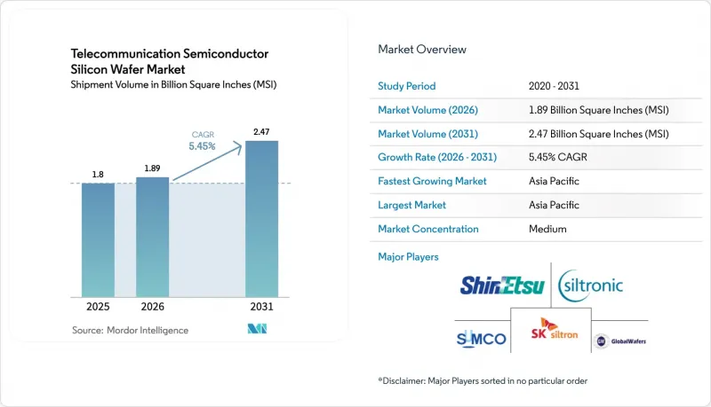
The Telecommunication Semiconductor Silicon Wafer Market size in terms of shipment volume is expected to grow from 1.8 Billion Square Inches (MSI) in 2025 to 1.89 Billion Square Inches (MSI) in 2026 and is forecast to reach 2.47 Billion Square Inches (MSI) by 2031 at 5.45% CAGR over 2026-2031.
An industry pivot toward 5G massive-MIMO base stations, early 6G research platforms, and silicon photonics transceivers is redefining substrate purity, diameter, and defect-density requirements. Government CHIPS-style incentives, particularly in the United States, the European Union, Japan, and South Korea, are encouraging domestic wafer-fab construction, shortening supply chains that were historically concentrated in East Asia. Consolidation among six global suppliers is reinforcing an oligopolistic pricing structure, while new Chinese entrants remain capacity-constrained by export controls on sub-14-nanometer equipment. At the same time, stricter environmental regulations on slurry waste and escalating capital intensity are putting pressure on cost structures, nudging the telecommunication semiconductor silicon wafer market toward higher value specialty substrates.
Global Telecommunication Semiconductor Silicon Wafer Market Trends and Insights
Surging 5G/6G Base-Station Deployments Demanding High-Purity 300 mm Wafers
Massive-MIMO base stations require gallium-nitride power amplifiers and silicon RF front-ends fabricated on 300 mm substrates that must exceed 1,000 ohm-centimeter resistivity to limit substrate losses at frequencies above 3.5 GHz. Global silicon wafer shipments climbed to 12.973 billion square inches in 2025, largely driven by telecom demand. Imec validated GaN-on-silicon RF transistors operating in the 7-24 GHz band, designated for 6G, extending wafer consumption beyond current 5G needs. China Mobile and China Telecom deployed a combined 1.2 million 5G sites by 2025, each using roughly 200-300 square inches of silicon. Only two suppliers consistently meet the parts-per-trillion metallic contamination threshold required for millimeter-wave applications.
Government CHIPS-Style Incentives Accelerating Telecom-Centric Wafer Fabs
The US CHIPS and Science Act reserved USD 36.4 billion across 40 projects by 2025, with GlobalWafers obtaining USD 400 million for twin 300 mm plants in Texas and Missouri. Texas Instruments secured USD 1.6 billion in funding, earmarked for four 300 mm fabs that feed base-station backhaul and power-supply ICs. Europe committed EUR 43 billion (USD 46 billion) under its Chips Act, underwriting Infineon and STMicroelectronics' capacity for RF and power wafers. Japan's JPY 920 billion (USD 6.2 billion) subsidy package is ensuring 300 mm substrate availability for 5G despite geopolitical frictions. These grants lower effective capital costs 25-35%, compressing payback times to under 10 years.
Capital Intensity and Long Payback Periods for 300 mm Wafer Lines
A single greenfield 300 mm plant costs USD 3-5 billion, with equipment absorbing up to 70% of outlay. Siltronic's Singapore expansion illustrates the challenge, spending EUR 2 billion (USD 2.14 billion) for 1 million wafers per year. Even entrenched firms like SUMCO and SK Siltron formed a joint venture to share a USD 3.6 billion build-out. Where subsidies cover less than 15% of costs, investors face 10-15 year payback horizons, deterring new entrants and reinforcing the oligopoly.
Other drivers and restraints analyzed in the detailed report include:
- Rapid Adoption of Silicon Photonics Transceivers Boosting SOI Wafer Demand
- Expansion of 300 mm Capacity for Cloud and Edge Data-Traffic Processors
- Defect-Density Challenges with High-Resistivity RF-Grade Wafers
For complete list of drivers and restraints, kindly check the Table Of Contents.
Segment Analysis
The 300 mm segment controlled 64.48% of volume in 2025, reflecting per-die savings of 30-40% and automation advantages. GlobalWafers' Sherman site shipped its first 1.2 million wafers in 2025, underscoring domestic momentum. Texas Instruments joined with four 40,000-wspm modules to feed analog and embedded telecom ICs. Equipment shortages keep 200 mm capacity tight, nudging redesigns onto 300 mm lines. Sub-150-mm wafers remain a niche for GaN power RF amplifiers and MEMS antenna tuners, yet continue to cede market share. Regulatory bodies have little sway over diameter choice, though export controls on 300 mm tools to China slow adoption there.
As chiplet architectures rise, each radio front-end now requires multiple dies across power, RF, and digital domains, inflating demand for larger substrates. The telecommunication semiconductor silicon wafer market sees suppliers bundling prime-polished and epitaxial variants to lock in volume. Industry consortia like SEMI standardize notch positions and thickness tolerances, allowing fabs to quickly qualify multiple sources, which tempers supplier power marginally but keeps barriers high for new entrants.
The Telecommunication Semiconductor Silicon Wafer Market Report is Segmented by Wafer Diameter (Up To 150 Mm, 200 Mm, and 300 Mm), Semiconductor Device Type (Logic, Memory, Analog, and More), Wafer Type (Prime Polished, Epitaxial, Silicon-On-Insulator (SOI), and More), and Geography. The Market Forecasts are Provided in Terms of Volume (Square Inches).
Geography Analysis
Asia-Pacific supplied 80.11% of wafers in 2025 and posts a 6.78% CAGR to 2031. China's 1.2 million 5G base stations create captive demand that domestic suppliers rush to serve, though tool embargoes keep yields below Japanese levels. Japan's Shin-Etsu and SUMCO together furnish about 55% of global 300 mm capacity, leveraging unmatched Czochralski expertise. South Korea's SUMCO-SK Siltron venture adds 1 million wafers annually by 2027, with telecom and automotive as anchor segments. Taiwan remains a voracious consumer through foundry leader TSMC, whose Kumamoto site secures JPY 920 billion (USD 6.2 billion) state backing.
North America gains momentum from USD 36.4 billion CHIPS Act funding. GlobalWafers and Texas Instruments collectively deliver 2 million 300 mm wafers by 2027, trimming reliance on Asian imports. Europe's EUR 43 billion (USD 46 billion) Chips Act bankrolls Infineon and STMicroelectronics expansions, yet its share lingers below 10% because of elevated energy and labor costs. South America and the Middle East and Africa remain small, importing wafers for limited 5G rollouts.
Export controls by the United States, Japan, and the Netherlands on sub-14 nm equipment fragment the Asia-Pacific chain, forcing Chinese fabs onto 28 nm and enlarging wafer area per function by up to 60%. China's retaliatory curbs on gallium and germanium raise compound-semiconductor costs, shifting demand to Japanese and Korean suppliers that enjoy diversified feedstock. Supply-chain diversification efforts will show material impact only after 2030 due to 10-15 year payback cycles for new fabs.
- Shin-Etsu Chemical Co., Ltd.
- SUMCO Corporation
- GlobalWafers Co., Ltd.
- Siltronic AG
- SK Siltron Co., Ltd.
- Soitec SA
- National Silicon Industry Group Co., Ltd.
- Wafer Works Corp.
- Hangzhou Semiconductor Wafer Co., Ltd.
- Ferrotec Holdings Corp.
- Okmetic Oyj
- MEMC Electronic Materials, Inc.
- Zhonghuan Semiconductor Co., Ltd.
- GRINM Semiconductor Materials Co., Ltd.
- Shanghai Advanced Silicon Technology Co., Ltd.
- MCL Electronic Materials Ltd.
- Simgui (Shanghai) Technology Co., Ltd.
- AST Photoelectricity Co., Ltd.
- LG Siltron Advanced Materials, Inc.
- NSIG (Shanghai) Silicon Technologies Co., Ltd.
Additional Benefits:
- The market estimate (ME) sheet in Excel format
- 3 months of analyst support
TABLE OF CONTENTS
1 INTRODUCTION
- 1.1 Study Assumptions and Market Definition
- 1.2 Scope of the Study
2 RESEARCH METHODOLOGY
3 EXECUTIVE SUMMARY
4 MARKET LANDSCAPE
- 4.1 Market Overview
- 4.2 Industry Value-Chain Analysis
- 4.3 Regulatory Landscape
- 4.4 Technology Analysis
- 4.5 Impact of Macroeconomic Factors on the Market
- 4.6 Porter's Five Forces Analysis
- 4.6.1 Bargaining Power of Suppliers
- 4.6.2 Bargaining Power of Buyers
- 4.6.3 Threat of New Entrants
- 4.6.4 Threat of Substitutes
- 4.6.5 Intensity of Competitive Rivalry
- 4.7 Market Drivers
- 4.7.1 Surging 5G/6G Base-Station Deployments Demanding High-Purity 300 mm Wafers
- 4.7.2 Government CHIPS-Style Incentives Accelerating Telecom-Centric Wafer Fabs
- 4.7.3 Rapid Adoption of Silicon Photonics Transceivers Boosting SOI Wafer Demand
- 4.7.4 Expansion of 300 mm Capacity for Cloud and Edge Data-Traffic Processors
- 4.7.5 Ultra-Thin Wafer Demand for Co-Packaged Optics Driving New Grinding Chemistries
- 4.7.6 Back-Side Power-Delivery Ready Wafers for AI-Powered Base-Station SoCs
- 4.8 Market Restraints
- 4.8.1 Capital Intensity and Long Payback Periods for 300 mm Wafer Lines
- 4.8.2 Defect-Density Challenges with High-Resistivity RF-Grade Wafers
- 4.8.3 Export-Control Restrictions on Advanced Wafer-Equipment Shipments
- 4.8.4 Stricter Slurry-Waste Regulations Impacting Photonics-Grade CMP Costs
5 MARKET SIZE AND GROWTH FORECASTS (VOLUME)
- 5.1 By Wafer Diameter
- 5.1.1 Up to 150 mm
- 5.1.2 200 mm
- 5.1.3 300 mm
- 5.2 By Semiconductor Device Type
- 5.2.1 Logic
- 5.2.2 Memory
- 5.2.3 Analog
- 5.2.4 Discrete
- 5.2.5 Other Semiconductor Device Types (Optoelectronics, Sensors, Micro)
- 5.3 By Wafer Type
- 5.3.1 Prime Polished
- 5.3.2 Epitaxial
- 5.3.3 Silicon-on-Insulator (SOI)
- 5.3.4 Specialty Silicon (High-Resistivity, Power, Sensor-Grade)
- 5.4 By Geography
- 5.4.1 North America
- 5.4.1.1 United States
- 5.4.1.2 Canada
- 5.4.1.3 Mexico
- 5.4.2 Europe
- 5.4.2.1 Germany
- 5.4.2.2 United Kingdom
- 5.4.2.3 France
- 5.4.2.4 Rest of Europe
- 5.4.3 Asia-Pacific
- 5.4.3.1 China
- 5.4.3.2 Japan
- 5.4.3.3 India
- 5.4.3.4 South Korea
- 5.4.3.5 Taiwan
- 5.4.3.6 Rest of Asia-Pacific
- 5.4.4 South America
- 5.4.5 Middle East
- 5.4.6 Africa
- 5.4.1 North America
6 COMPETITIVE LANDSCAPE
- 6.1 Market Concentration
- 6.2 Strategic Moves
- 6.3 Market Share Analysis
- 6.4 Company Profiles (includes Global Level Overview, Market Level Overview, Core Segments, Financials as available, Strategic Information, Market Rank/Share, Products and Services, Recent Developments)
- 6.4.1 Shin-Etsu Chemical Co., Ltd.
- 6.4.2 SUMCO Corporation
- 6.4.3 GlobalWafers Co., Ltd.
- 6.4.4 Siltronic AG
- 6.4.5 SK Siltron Co., Ltd.
- 6.4.6 Soitec SA
- 6.4.7 National Silicon Industry Group Co., Ltd.
- 6.4.8 Wafer Works Corp.
- 6.4.9 Hangzhou Semiconductor Wafer Co., Ltd.
- 6.4.10 Ferrotec Holdings Corp.
- 6.4.11 Okmetic Oyj
- 6.4.12 MEMC Electronic Materials, Inc.
- 6.4.13 Zhonghuan Semiconductor Co., Ltd.
- 6.4.14 GRINM Semiconductor Materials Co., Ltd.
- 6.4.15 Shanghai Advanced Silicon Technology Co., Ltd.
- 6.4.16 MCL Electronic Materials Ltd.
- 6.4.17 Simgui (Shanghai) Technology Co., Ltd.
- 6.4.18 AST Photoelectricity Co., Ltd.
- 6.4.19 LG Siltron Advanced Materials, Inc.
- 6.4.20 NSIG (Shanghai) Silicon Technologies Co., Ltd.
7 MARKET OPPORTUNITIES AND FUTURE OUTLOOK
- 7.1 White-Space and Unmet-Need Assessment

