
PUBLISHER: Mordor Intelligence | PRODUCT CODE: 2044008

PUBLISHER: Mordor Intelligence | PRODUCT CODE: 2044008
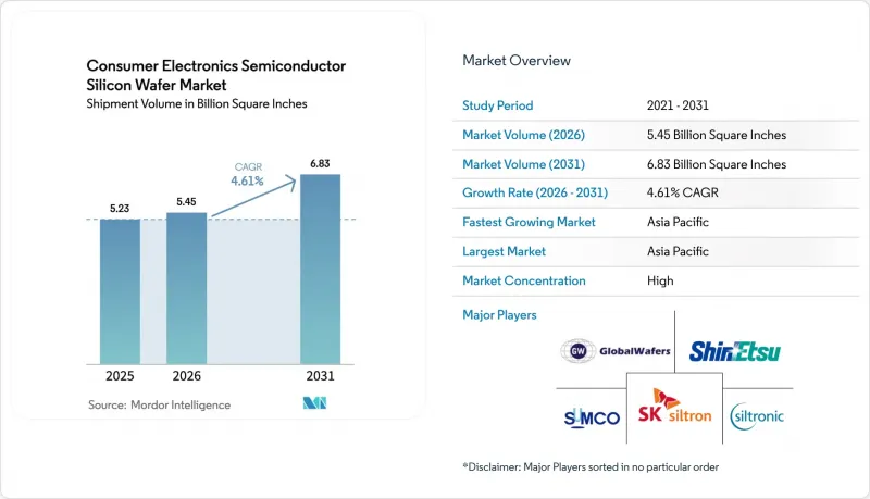
Consumer Electronics Semiconductor Silicon Wafer - Market Share Analysis, Industry Trends & Statistics, Growth Forecasts (2026 - 2031)
The Consumer Electronics Semiconductor Silicon Wafer Market size in terms of shipment volume is projected to expand from 5.23 Billion Square Inches in 2025 and 5.45 Billion Square Inches in 2026 to 6.83 Billion Square Inches by 2031, registering a CAGR of 4.61% between 2026 to 2031.
Strengthening demand for logic-intensive devices, migration to advanced node geometries, and government-backed fab incentives anchor this growth. Capital outlays by leading foundries continue to favor 300 mm substrates that maximize die counts, while specialty wafers such as silicon-on-insulator (SOI) gain share because they enable higher radio-frequency efficiency in 5G smartphones. Conversely, trailing-edge 200 mm capacity faces enduring margin pressure as analog and discrete devices remain on mature nodes. Regional diversification efforts in the United States and Europe are underway, yet Asia-Pacific retains its structural advantage in cost, existing supply chains, and installed wafer capacity.
Global Consumer Electronics Semiconductor Silicon Wafer Market Trends and Insights
Proliferation of 5G-Enabled Smartphones
Handset vendors embed multiple sub-6 GHz and millimeter-wave front-end modules, each containing discrete dies for low-noise and power amplifiers. Qualcomm's Snapdragon 8 Elite, fabricated on an advanced 4 nm process, allocates roughly 30% more wafer area per device than previous LTE platforms. Stand-alone 5G networks are rolling out in China and India, sustaining wafer pull-through even as global unit shipments plateau. Radio-frequency SOI substrates mitigate signal loss, enabling premium pricing that supports the 5.31% CAGR for SOI wafers. Partial substitution by gallium-nitride and indium-phosphide amplifiers tempers, but does not derail, incremental silicon demand.
Growth in High-Capacity Mobile Storage (3D NAND)
Smartphones equipped with 512 GB and 1 TB tiers accelerated a shift to 232-layer NAND stacks, increasing wafer starts and rework cycles. Reported shortages in late 2025 drove an earlier adoption of 1 Tb die schemes, raising silicon consumption per terabyte shipped. Concurrently, Samsung and SK hynix redirected 300 mm lines toward high-bandwidth memory, constricting consumer-grade NAND supply and lifting wafer average selling prices. The resulting demand spike peaks within two years as yield learning curves mature and new capacity comes online.
Capital-Intensive Large-Diameter Crystal Growth
A single 300 mm Czochralski line can exceed USD 400 million when factoring in pullers, slicing saws, and metrology. Equipment lead times often surpass two years, delaying new capacity during cyclical upswings. Siltronic's mid-single-digit revenue decline outlook for 2026 underscores how prolonged inventory digestion and deferred capex amplify fixed-cost exposure. SUMCO's planned closure of its Miyazaki 200 mm plant by the end of 2026 reflects legacy overcapacity and the capital burden of retooling. Higher labor and energy costs in North America and Europe further elevate breakeven thresholds, tightening this restraint.
Other drivers and restraints analyzed in the detailed report include:
- Expansion of Consumer IoT and Wearables
- Government Incentives for Domestic Logic Fabs
- Carbon-Footprint Caps from Consumer OEMs
For complete list of drivers and restraints, kindly check the Table Of Contents.
Segment Analysis
The 300 mm class captured 71.29% of the consumer electronics semiconductor silicon wafer market share in 2025, reflecting superior die-per-wafer economics that outweigh higher tool costs. This segment follows a growth curve aligned with the overall 4.61% CAGR as foundries channel record capex toward 3 nm and gate-all-around nodes. TSMC alone earmarked USD 52-56 billion for 2026 expansions, nearly all of which were devoted to 300 mm fabs. The consumer electronics semiconductor silicon wafer market size for 300 mm platforms is poised to reach 4,900 million square inches by 2031.
Emerging thinning and bonding techniques enable 300 mm substrates below 50 µm, unlocking applications once restricted to smaller diameters. Meanwhile, 200 mm lines persist for analog, MEMS, and power discretes, where process migration delivers limited benefit. Sub-150-mm wafers are receding to niche roles, chiefly high-resistivity RF switches and specialty sensors. Supply rationalization, including SUMCO's Miyazaki shutdown, helps stabilize pricing for legacy nodes even as premium 300 mm output scales.
The Consumer Electronics Semiconductor Silicon Wafer Market Report is Segmented by Wafer Diameter (Up To 150 Mm, 200 Mm, 300 Mm), Semiconductor Device Type (Logic, Memory, and More), Wafer Type (Prime Polished, Epitaxial, Specialty Silicon, and More), and Geography (North America, Europe, Asia-Pacific, South America, Middle East, Africa). The Market Forecasts are Provided in Terms of Shipment Volume (Square Inches).
Geography Analysis
Asia-Pacific led the consumer electronics semiconductor silicon wafer market share with 84.78% of 2025 volume and is advancing at a 5.78% CAGR through 2031. The region benefits from deep supply chains in Taiwan, South Korea, Japan, and China, each supported by multi-billion-dollar incentives for advanced logic fabs. TSMC's heavy 2026 capital program and China's goal of holding one-quarter of global 12-inch capacity further anchor demand. South Korean firms are pivoting 300 mm lines to high-bandwidth memory, tightening local supply for commodity NAND. India's USD 10 billion semiconductor mission brings new proposals, yet wafer production there still relies on imports.
North America is growing from a low base as the CHIPS and Science Act channels USD 36.4 billion into fab construction. TSMC's Arizona complex and Intel's Ohio project will stimulate local substrate pull once high-volume manufacturing begins in 2027. GlobalWafers plans the first U.S. 300 mm wafer plant in two decades, but higher labor and power costs temper its cost position. Europe mobilized EUR 80 billion under the EU Chips Act, focusing on analog and power devices in Germany and France. Siltronic's revenue outlook points to continued inventory digestion, yet regional funding should slow the talent drain to Asia.
South America, the Middle East, and Africa together account for only a sliver of the consumer electronics semiconductor silicon wafer market size because they lack large crystal-growth facilities. These regions depend on imports from Asia and, to a lesser extent, Europe and the United States. Global ISO 9001 and ISO 14001 standards maintain product quality consistency, but geographic concentration still exposes the supply chain to natural disasters and geopolitical tensions.
- Shin-Etsu Chemical Co., Ltd.
- SUMCO Corporation
- GlobalWafers Co., Ltd.
- Siltronic AG
- SK siltron Co., Ltd.
- Soitec S.A.
- National Silicon Industry Group Co., Ltd.
- Wafer Works Corp.
- Okmetic Oy
- Ferrotec Holdings Corporation
- Hebei Puxing Electronic Technology Co., Ltd.
- Zhonghuan Semiconductor Co., Ltd.
- Hangzhou Semiconductor Wafer Co., Ltd.
- GRINM Semiconductor Materials Co., Ltd.
- MCL Electronic Materials Co., Ltd.
- Shanghai Simgui Technology Co., Ltd.
- Virginia Semiconductor, Inc.
- Silicon Valley Microelectronics, Inc.
- Topsil Semiconductor Materials A/S
- Silicon Materials, Inc.
Additional Benefits:
- The market estimate (ME) sheet in Excel format
- 3 months of analyst support
TABLE OF CONTENTS
1 INTRODUCTION
- 1.1 Study Assumptions and Market Definition
- 1.2 Scope of the Study
2 RESEARCH METHODOLOGY
3 EXECUTIVE SUMMARY
4 MARKET LANDSCAPE
- 4.1 Market Overview
- 4.2 Market Drivers
- 4.2.1 Proliferation of 5G-Enabled Smartphones
- 4.2.2 Growth in High-Capacity Mobile Storage (3D NAND)
- 4.2.3 Expansion of Consumer IoT and Wearables
- 4.2.4 Government Incentives for Domestic Logic Fabs
- 4.2.5 Adoption of TSV Interposers in AR/VR Headsets
- 4.2.6 Silicon Photonics Uptake in XR Devices
- 4.3 Market Restraints
- 4.3.1 Capital-Intensive Large-Diameter Crystal Growth
- 4.3.2 Supply Constraints of High-Purity Polysilicon
- 4.3.3 Shift of RF Modules to Compound Substrates
- 4.3.4 Carbon-Footprint Caps from Consumer OEMs
- 4.4 Industry Value Chain Analysis
- 4.5 Regulatory Landscape
- 4.6 Technology Analysis
- 4.7 Impact of Macroeconomic Factors on the Market
- 4.8 Porter's Five Forces Analysis
- 4.8.1 Bargaining Power of Suppliers
- 4.8.2 Bargaining Power of Buyers
- 4.8.3 Threat of New Entrants
- 4.8.4 Threat of Substitutes
- 4.8.5 Intensity of Competitive Rivalry
5 MARKET SIZE AND GROWTH FORECASTS (VOLUME)
- 5.1 By Wafer Diameter
- 5.1.1 Up to 150 mm
- 5.1.2 200 mm
- 5.1.3 300 mm
- 5.2 By Semiconductor Device Type
- 5.2.1 Logic
- 5.2.2 Memory
- 5.2.3 Analog
- 5.2.4 Discrete
- 5.2.5 Other Semiconductor Device Types (Optoelectronics, Sensors, Micro)
- 5.3 By Wafer Type
- 5.3.1 Prime Polished
- 5.3.2 Epitaxial
- 5.3.3 Silicon-on-Insulator (SOI)
- 5.3.4 Specialty Silicon (High-Resistivity, Power, Sensor-Grade)
- 5.4 By Geography
- 5.4.1 North America
- 5.4.1.1 United States
- 5.4.1.2 Canada
- 5.4.1.3 Mexico
- 5.4.2 Europe
- 5.4.2.1 Germany
- 5.4.2.2 United Kingdom
- 5.4.2.3 France
- 5.4.2.4 Rest of Europe
- 5.4.3 Asia-Pacific
- 5.4.3.1 China
- 5.4.3.2 Japan
- 5.4.3.3 India
- 5.4.3.4 South Korea
- 5.4.3.5 Taiwan
- 5.4.3.6 Rest of Asia-Pacific
- 5.4.4 South America
- 5.4.5 Middle East
- 5.4.6 Africa
- 5.4.1 North America
6 COMPETITIVE LANDSCAPE
- 6.1 Market Concentration
- 6.2 Strategic Moves
- 6.3 Market Share Analysis
- 6.4 Company Profiles (includes Global Level Overview, Market Level Overview, Core Segments, Financials as available, Strategic Information, Market Rank/Share, Products and Services, Recent Developments)
- 6.4.1 Shin-Etsu Chemical Co., Ltd.
- 6.4.2 SUMCO Corporation
- 6.4.3 GlobalWafers Co., Ltd.
- 6.4.4 Siltronic AG
- 6.4.5 SK siltron Co., Ltd.
- 6.4.6 Soitec S.A.
- 6.4.7 National Silicon Industry Group Co., Ltd.
- 6.4.8 Wafer Works Corp.
- 6.4.9 Okmetic Oy
- 6.4.10 Ferrotec Holdings Corporation
- 6.4.11 Hebei Puxing Electronic Technology Co., Ltd.
- 6.4.12 Zhonghuan Semiconductor Co., Ltd.
- 6.4.13 Hangzhou Semiconductor Wafer Co., Ltd.
- 6.4.14 GRINM Semiconductor Materials Co., Ltd.
- 6.4.15 MCL Electronic Materials Co., Ltd.
- 6.4.16 Shanghai Simgui Technology Co., Ltd.
- 6.4.17 Virginia Semiconductor, Inc.
- 6.4.18 Silicon Valley Microelectronics, Inc.
- 6.4.19 Topsil Semiconductor Materials A/S
- 6.4.20 Silicon Materials, Inc.
7 MARKET OPPORTUNITIES AND FUTURE OUTLOOK
- 7.1 White-Space and Unmet-Need Assessment

