
PUBLISHER: Mordor Intelligence | PRODUCT CODE: 2044018

PUBLISHER: Mordor Intelligence | PRODUCT CODE: 2044018
Semiconductor Wafer Reclaim - Market Share Analysis, Industry Trends & Statistics, Growth Forecasts (2026 - 2031)
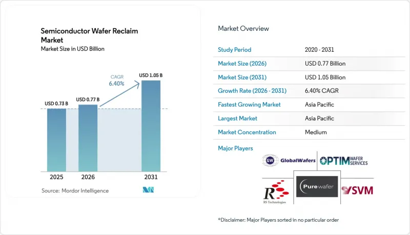
The semiconductor wafer reclaim market size was valued at USD 0.73 billion in 2025 and estimated to grow from USD 0.77 billion in 2026 to reach USD 1.05 billion by 2031, at a CAGR of 6.4% during the forecast period (2026-2031).
Heightened capital intensity at advanced nodes, paired with regulatory requirements for circular manufacturing, is steering integrated device manufacturers toward reclaimed substrates. The shift lowers total cost of ownership for test and monitor wafers, trims carbon footprints, and buffers supply-chain risk as virgin-wafer pricing stays volatile. Artificial-intelligence-driven inspection now compresses turnaround from days to hours, letting reclaim vendors match the cadence of high-volume fabs. Meanwhile, Asia-Pacific's dense 300 mm fab cluster anchors demand, while emerging silicon-carbide and gallium-nitride pilot lines open white-space opportunities in compound-semiconductor reclaim. Competitive intensity remains moderate because the chemical-mechanical polishing and metrology infrastructure required for yields above 95% creates natural entry barriers.
Global Semiconductor Wafer Reclaim Market Trends and Insights
Expanding 300 mm Fab Capacity In Asia-Pacific
Asia-Pacific is set to add the bulk of new 300 mm lines through 2027, lifting baseline demand for reclaimed test wafers that account for 15%-20% of every fab's monthly starts. New plants in Singapore and Taiwan add more than 2 million wafer starts per month, each of which can be reused five to seven times when reclaimed, driving volume elasticity for the semiconductor wafer reclaim market. Dense regional clustering also trims logistics to sub-48-hour cycles, aligning reclaim supply with just-in-time production schedules. Vendors are therefore co-locating facilities near megafabs, locking in multiyear contracts that stabilize cash flow. As additional capacity ramps, reclaim ceases to be a tactical cost lever and becomes a structural component of fab planning.
Cost-Optimization Pressure On Test And Monitor Wafers
Virgin test wafers now cost USD 120-USD 150 per 300 mm piece, up 18% since 2024, pinching gross margins for logic, memory, and power fabs. Reclaimed substrates drop the effective cost to USD 25-USD 35 after five to eight cycles, yielding immediate savings. Large foundries have validated that reclaimed monitor wafers meet metrology precision without yield loss. Device makers are also deploying machine-learning models to predict remaining reclaim cycles, ensuring wafers retire only when surface roughness limits approach critical thresholds. The economic case is strongest at mature nodes, but even 5 nm facilities now reclaim wafers for non-device steps such as chamber seasoning.
Stringent Surface-Defect Specs For 2 nm Node
Gate-all-around transistors at 2 nm demand surface-defect densities below 0.1 defects per cm2, a level reclaim processes struggle to guarantee after multiple polish cycles. The need for atomic-layer cleansing steps adds USD 15-USD 20 per wafer, eroding savings and confining reclaimed wafers to non-critical steps in advanced-node fabs. Until vendors demonstrate repeatable sub-0.1 nm flatness, leading-edge logic lines will cap reclaim penetration, limiting upside in the most valuable segment of the semiconductor wafer reclaim market.
Other drivers and restraints analyzed in the detailed report include:
- Sustainability Regulations Favoring Circular-Economy Practices
- AI-Enabled Yield-Imaging Tools Boosting Reclaim Yields
- Limited Skilled Labor For Advanced Polishing Lines
For complete list of drivers and restraints, kindly check the Table Of Contents.
Segment Analysis
The 300 mm format accounted for 52.84% of 2025 revenue, anchoring the semiconductor wafer reclaim market size for logic and memory fabs. Yet the 200 mm segment is forecast to rise at 7.28% during 2026-2031, outpacing all other diameters. Automotive and industrial players continue to favor mature nodes for power-management ICs and micro-electromechanical systems, applications that map efficiently onto 200 mm tooling. New silicon-carbide pilot lines at this diameter further widen the addressable base. Reclaim vendors retrofit legacy polishers with endpoint-detection sensors, delivering sub-nanometer control while preserving fully depreciated equipment, which lifts margins without heavy capital outlays. As electrification accelerates, 200 mm reclaim volume will narrow the revenue gap with 300 mm lines even though the latter retains absolute leadership.
Demand for 150 mm reclaim persists in niche aerospace and radiation-hardened circuits, aided by satellite constellations that prefer smaller diameters for cost control on specialized die. Compound-semiconductor substrates often debut at 150 mm before scaling, giving vendors an entry path into future wide-bandgap demand. Collectively, the diameter mix underscores how the semiconductor wafer reclaim market shifts with end-application economics, not just Moore's Law progression. Vendors diversified across 150 mm through 300 mm lines hedge exposure to any single technology cycle and capture step-wise growth as each diameter finds renewed relevance.
The Semiconductor Wafer Reclaim Market Report is Segmented by Wafer Diameter (Up To 150 Mm, 200 Mm, and More), Wafer Type (Test and Monitor Wafer Reclaim, Prime Wafer Reclaim, Epitaxial Wafer Reclaim, and More), Device Manufacturing Category (Memory Devices, Logic Devices, Analog and Power Devices, and More), and Geography. The Market Forecasts are Provided in Terms of Value (USD).
Geography Analysis
Asia-Pacific generated 63.79% of 2025 revenue and grows at 6.92% through 2031, powered by Taiwan, South Korea, China, and Singapore, which together host more than two-thirds of global 300 mm capacity. Co-location strategies shrink wafer-transit time to less than two days, lowering work-in-process inventory for fabs and cementing reclaim as an operational staple. China's dual-circulation policy further accelerates domestic reclaim capacity, treating local suppliers as a buffer against geopolitical shocks and export controls.
North America captured about 18% of 2025 turnover, but CHIPS Act subsidies are now spawning greenfield fabs from Arizona to Texas. New plants integrate reclaim bays at inception, reflecting circular-economy design principles embedded in funding guidelines. Skilled-labor shortages remain a drag, yet community-college certificate programs are beginning to close the gap, suggesting a medium-term uplift in regional capacity additions and cementing demand for the semiconductor wafer reclaim market in the United States.
Europe held roughly 12% of revenue in 2025, with the EU Chips Act mandating reclaimed-silicon quotas that underpin vendor order books. Co-located operations in Italy and Austria combine virgin and reclaim under one roof, trimming logistics emissions and satisfying regulators. Rest of World countries account for the balance, with Israel's mature microelectronics cluster and nascent Middle East fab proposals likely to seed incremental demand post-2028. Geography dynamics therefore track fab investments rather than end-market consumption, concentrating growth where capital flows into new wafer starts.
- RS Technologies Co., Ltd.
- Pure Wafer, Inc.
- GlobalWafers Co., Ltd.
- Optim Wafer Services Ltd.
- Silicon Valley Microelectronics, Inc.
- Phoenix Silicon International Corp.
- NanoSILICON, Inc.
- ReSilicon Group LLC
- Kay M Analytics Pte Ltd.
- Siltronic AG
- SUMCO Corporation
- Wafer World, Inc.
- Noel Technologies, Inc.
- PSEMI Corporation
- SiWave Technologies GmbH
- MicroTech Systems, Inc.
- WaferNET, Inc.
- Silicon Materials, Inc.
- REC Silicon ASA
- SilRec S.p.A.
Additional Benefits:
- The market estimate (ME) sheet in Excel format
- 3 months of analyst support
TABLE OF CONTENTS
1 INTRODUCTION
- 1.1 Study Assumptions and Market Definition
- 1.2 Scope of the Study
2 RESEARCH METHODOLOGY
3 EXECUTIVE SUMMARY
4 MARKET LANDSCAPE
- 4.1 Market Overview
- 4.2 Market Drivers
- 4.2.1 Expanding 300 mm Fab Capacity in Asia-Pacific
- 4.2.2 Cost-Optimisation Pressure on Test and Monitor Wafers
- 4.2.3 Sustainability Regulations Favouring Circular-Economy Practices
- 4.2.4 AI-Enabled Yield-Imaging Tools Boosting Reclaim Yields (Under-the-Radar)
- 4.2.5 Secondary-Market Demand from Low-Earth-Orbit Satellites (Under-the-Radar)
- 4.2.6 Foundry Shift to SiC/GaN Pilot Wafers Requiring Reclaim (Under-the-Radar)
- 4.3 Market Restraints
- 4.3.1 Stringent Surface-Defect Specs for 2 nm Node
- 4.3.2 Limited Skilled Labour for Advanced Polishing Lines
- 4.3.3 Uncertain Scrap-Silicon Pricing Volatility (Under-the-Radar)
- 4.3.4 Cyber-Security Risks in Fab-to-Reclaim Logistics (Under-the-Radar)
- 4.4 Impact of Macroeconomic Factors on the Market
- 4.5 Industry Value-Chain Analysis
- 4.6 Regulatory Landscape
- 4.7 Technological Outlook
- 4.8 Porter's Five Forces Analysis
- 4.8.1 Threat of New Entrants
- 4.8.2 Bargaining Power of Suppliers
- 4.8.3 Bargaining Power of Buyers
- 4.8.4 Threat of Substitutes
- 4.8.5 Intensity of Competitive Rivalry
5 MARKET SIZE AND GROWTH FORECASTS (VOLUME)
- 5.1 By Wafer Diameter
- 5.1.1 150 mm
- 5.1.2 200 mm
- 5.1.3 300 mm
- 5.2 By Wafer Type
- 5.2.1 Test and Monitor Wafer Reclaim
- 5.2.2 Prime Wafer Reclaim
- 5.2.3 Epitaxial Wafer Reclaim
- 5.2.4 SOI Wafer Reclaim
- 5.3 By Device Manufacturing Category
- 5.3.1 Memory Devices
- 5.3.2 Logic Devices
- 5.3.3 Analog and Power Devices
- 5.3.4 Specialty Devices (MEMS, Sensors, RF)
- 5.3.5 R&D Facilities
- 5.4 By Geography
- 5.4.1 North America
- 5.4.2 Europe
- 5.4.3 Asia-Pacific
- 5.4.4 Rest of the World
6 COMPETITIVE LANDSCAPE
- 6.1 Market Concentration
- 6.2 Strategic Moves
- 6.3 Market Share Analysis
- 6.4 Company Profiles (includes Global Level Overview, Market Level Overview, Core Segments, Financials as available, Strategic Information, Market Rank/Share, Products and Services, Recent Developments)
- 6.4.1 RS Technologies Co., Ltd.
- 6.4.2 Pure Wafer, Inc.
- 6.4.3 GlobalWafers Co., Ltd.
- 6.4.4 Optim Wafer Services Ltd.
- 6.4.5 Silicon Valley Microelectronics, Inc.
- 6.4.6 Phoenix Silicon International Corp.
- 6.4.7 NanoSILICON, Inc.
- 6.4.8 ReSilicon Group LLC
- 6.4.9 Kay M Analytics Pte Ltd.
- 6.4.10 Siltronic AG
- 6.4.11 SUMCO Corporation
- 6.4.12 Wafer World, Inc.
- 6.4.13 Noel Technologies, Inc.
- 6.4.14 PSEMI Corporation
- 6.4.15 SiWave Technologies GmbH
- 6.4.16 MicroTech Systems, Inc.
- 6.4.17 WaferNET, Inc.
- 6.4.18 Silicon Materials, Inc.
- 6.4.19 REC Silicon ASA
- 6.4.20 SilRec S.p.A.
7 MARKET OPPORTUNITIES AND FUTURE OUTLOOK
- 7.1 White-Space And Unmet-Need Assessment

