
PUBLISHER: Mordor Intelligence | PRODUCT CODE: 2062042

PUBLISHER: Mordor Intelligence | PRODUCT CODE: 2062042
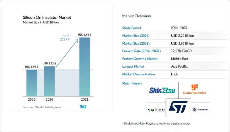
Silicon On Insulator - Market Share Analysis, Industry Trends & Statistics, Growth Forecasts (2026 - 2031)
According to Mordor Intelligence, the silicon-on-insulator market size was valued at USD 1.96 billion in 2025 and is estimated to grow from USD 2.22 billion in 2026 to USD 3.96 billion by 2031, at a CAGR of 12.27% during the forecast period (2026-2031).
This report is Segmented by SOI Platform (FD-SOI, PD-SOI, Power-SOI, and Other SOI Platforms), Wafer Size (≤200 Mm, and ≥201 Mm), Technology (Bonding SOI, and More), Application (MEMS, Power Supplies, Optical Communication, and More), End-User Vertical (Consumer Electronics, Automotive, IT and Telecommunication, and More), and Geography. The Market Forecasts are Provided in Terms of Value (USD).
Global Silicon On Insulator Market Trends and Insights
Expanding Adoption of FD-SOI in 5G RF Front-End Modules
Smartphone radio architectures integrate more power amplifiers, switches, and tuners to support carrier aggregation, with FD-SOI providing required linearity and harmonic suppression without costlier substrates. RF-SOI wafer shipments grew significantly in 2025 as multi-band flagships launched. Foundries now produce 22 nm FD-SOI nodes for radio applications, combining analog, digital, and power blocks on a single die to reduce PCB footprints. 3GPP Release 18 standards, met by FD-SOI through real-time back-biasing, further drive wafer demand, boosting the silicon-on-insulator market. FD-SOI is also being adopted for massive-MIMO radios, expanding growth beyond handsets.
Growing Demand for High-Performance, Low-Power Edge AI Chips
Edge inference engines in vehicles, cameras, and wearables must meet milliwatt standby budgets while delivering tera-operations-per-second performance. FD-SOI's ultra-thin body reduces leakage and supports operation down to 0.4 V, driving automotive AI SoCs to adopt 28 nm FD-SOI platforms in 2025. Engineers use back-bias to manage temperature swings from -40 °C to 125 °C, meeting safety mandates without adding guard-band voltage. Standardizing this approach increases wafer volume, lowers costs, and boosts adoption, expanding the silicon-on-insulator market.
Supply-Demand Imbalance in 300 mm SOI Wafer Capacity
By 2025, only one high-volume 300 mm line reached scale, with expansions delayed until late 2027. Foundries face wafer costs 20%-30% higher than those for bulk silicon, squeezing margins and slowing migration to larger diameters. Some fabless customers shifted to 200 mm nodes to secure supply, but this diluted volumes and delayed cost curves, limiting near-term SOI market growth. Bulk-silicon giants remain cautious about SOI capex due to tighter thickness control and the higher capital intensity required for 300 mm hydrogen-implantation steps. Short-term dual-sourcing remedies raise engineering overhead, providing only partial relief.
Other drivers and restraints analyzed in the detailed report include:
- Governments' Strategic Semiconductor Sovereignty Initiatives
- Electric-Vehicle Powertrain Efficiency Improvements Using Power-SOI
- High Fabrication Cost Versus Bulk Silicon Alternatives
For complete list of drivers and restraints, kindly check the Table Of Contents.
Segment Analysis
The 54.21% revenue share held by FD-SOI in 2025 was the largest slice of the silicon-on-insulator market, buoyed by widespread deployment in RF transceivers, low-power microcontrollers, and consumer wearables. OEMs selected the platform for its ability to operate below 0.5 V while still delivering the gain linearity and noise margins demanded by next-generation radios. The silicon-on-insulator market size for Power-SOI is projected to grow at a 13.07% CAGR between 2026 and
At the process-technology level, GlobalFoundries' 22 nm FD-SOI node recorded more than 50 automotive tape-outs by year-end 2025, confirming robust design-win momentum. STMicroelectronics and Samsung Foundry continue to proliferate FD-SOI across analog and mixed-signal catalogs, whereas Infineon and ON Semiconductor channel R&D toward Power-SOI for 800 V drive trains. This platform bifurcation enables wafer suppliers to fine-tune box and handle layers for application-specific needs, deepening value capture across the silicon-on-insulator industry.
Substrates measuring 201 mm or more captured 68.33% of 2025 revenue, reflecting die-per-wafer leverage that cuts costs by roughly one-third once volume reaches steady state. Most foundries are positioning 300 mm SOI lines in Europe and North America under government-backed subsidy programs, further anchoring this segment of the silicon-on-insulator market. However, Smart Cut at 300 mm demands sub-nanometer thickness uniformity; yield excursions therefore ripple quickly across hundreds of dies, underscoring the strategic importance of announced capacity increases.
Smaller diameters retain vitality in MEMS microphones, gyro sensors, and integrated photonics, where die footprints cap out far below a full reticle. Okmetic and Wafer Works maintain profitable niches in 150 mm and 200 mm runs, using faster cycle times to iterate alongside start-ups. Such capacity provides a relief valve, as designers hedge against the tight supply of 300 mm blanks, preserving resilience across the broader silicon-on-insulator market.
Geography Analysis
Asia-Pacific commanded 46.83% of global revenue in 2025, anchored by China's indigenous foundry surge and Japan's enduring edge in precision MEMS fabrication. Taiwan and South Korea add depth through leading-edge logic and memory, while India's Production-Linked Incentive scheme is drawing assembly and test investments that will back-propagate wafer demand. Regional build-outs in 5G base stations and edge AI gateways further multiply consumption of FD-SOI and Power-SOI substrates.
North America combines sovereign-funded fab projects with long-standing aerospace and defense applications that value SOI for radiation hardness. Intel, GlobalFoundries, and TSMC have each broken ground on U.S. facilities slated to consume 300-mm specialty wafers when ramping begins in 2027. Europe follows closely, supported by EUR 43 billion (USD 48.4 billion) in Chips Act incentives that target automotive and industrial semiconductors. STMicroelectronics, Infineon, and NXP are already integrating localized SOI capacity into their roadmap to de-risk supply.
The Middle East represents the most dynamic frontier, with sovereign wealth funds allocating multibillion-dollar capital pools to semiconductor fabs focused on optical interconnects and AI accelerators. Pilot lines in the United Arab Emirates and Saudi Arabia plan to leverage SOI photonics to lower data-center energy intensity, reinforcing a 13.21% CAGR outlook for the region. South America and Africa are early in ecosystem development; nonetheless, pilot programs in Brazil and South Africa signal future upside for the silicon on insulator market as policy frameworks mature.
- Soitec SA
- Shin-Etsu Chemical Co., Ltd.
- GlobalWafers Co., Ltd.
- GlobalFoundries Inc.
- STMicroelectronics N.V.
- NXP Semiconductors N.V.
- Samsung Electronics Co., Ltd.
- Taiwan Semiconductor Manufacturing Company Limited
- Intel Corporation
- Siltronic AG
- SUMCO Corporation
- Okmetic Oyj
- Wafer Works Corporation
- NTT Advanced Technology Corporation
- China Silicon Corporation
- Skyworks Solutions, Inc.
- Infineon Technologies AG
- Murata Manufacturing Co., Ltd.
- Advanced Micro Devices, Inc.
- Analog Devices, Inc.
Additional Benefits:
- The market estimate (ME) sheet in Excel format
- 3 months of analyst support
TABLE OF CONTENTS
1 INTRODUCTION
- 1.1 Study Assumptions and Market Definition
- 1.2 Scope of the Study
2 RESEARCH METHODOLOGY
3 EXECUTIVE SUMMARY
4 MARKET LANDSCAPE
- 4.1 Market Overview
- 4.2 Market Drivers
- 4.2.1 Expanding Adoption of FD-SOI in 5G RF Front-End Modules
- 4.2.2 Growing Demand for High-Performance, Low-Power Edge AI Chips
- 4.2.3 Governments' Strategic Semiconductor Sovereignty Initiatives
- 4.2.4 Electric Vehicle Powertrain Efficiency Improvements Using Power-SOI
- 4.2.5 Rising Use of MEMS Sensors in Smart Industry 4.0 Applications
- 4.2.6 Surge in Optical Interconnects for Data Centers Leveraging SOI Photonics
- 4.3 Market Restraints
- 4.3.1 Supply-Demand Imbalance in 300 mm SOI Wafer Capacity
- 4.3.2 High Fabrication Cost Versus Bulk Silicon Alternatives
- 4.3.3 Complexity of Integrating SOI with Advanced Packaging Technologies
- 4.3.4 IP Ownership and Licensing Barriers in Smart Cut Process
- 4.4 Impact of Macroeconomic Factors on the Market
- 4.5 Industry Value Chain Analysis
- 4.6 Regulatory Landscape
- 4.7 Technological Outlook
- 4.8 Porter's Five Forces Analysis
- 4.8.1 Bargaining Power of Suppliers
- 4.8.2 Bargaining Power of Buyers
- 4.8.3 Threat of New Entrants
- 4.8.4 Threat of Substitutes
- 4.8.5 Intensity of Competitive Rivalry
5 MARKET SIZE AND GROWTH FORECASTS (VALUE)
- 5.1 By SOI Platform
- 5.1.1 Fully Depleted Silicon on Insulator (FD-SOI)
- 5.1.2 Partially Depleted Silicon on Insulator (PD-SOI)
- 5.1.3 Power-SOI
- 5.1.4 Other Types
- 5.2 By Wafer Size
- 5.2.1 Less Than or Equal To 200 mm
- 5.2.2 201 mm and Above
- 5.3 By Technology
- 5.3.1 Bonding SOI
- 5.3.2 Layer Transfer SOI
- 5.3.3 Smart Cut
- 5.4 By Application
- 5.4.1 MEMS
- 5.4.2 Power Supplies
- 5.4.3 Optical Communication
- 5.4.4 Image Sensing
- 5.4.5 Other Applications
- 5.5 By End-User Vertical
- 5.5.1 Consumer Electronics
- 5.5.2 Automotive
- 5.5.3 IT and Telecommunication
- 5.5.4 Aerospace and Defense
- 5.5.5 Industrial
- 5.5.6 Other End User Verticals
- 5.6 By Geography
- 5.6.1 North America
- 5.6.1.1 United States
- 5.6.1.2 Canada
- 5.6.1.3 Mexico
- 5.6.2 South America
- 5.6.2.1 Brazil
- 5.6.2.2 Argentina
- 5.6.2.3 Rest of South America
- 5.6.3 Europe
- 5.6.3.1 United Kingdom
- 5.6.3.2 Germany
- 5.6.3.3 France
- 5.6.3.4 Italy
- 5.6.3.5 Rest of Europe
- 5.6.4 Asia-Pacific
- 5.6.4.1 China
- 5.6.4.2 Japan
- 5.6.4.3 India
- 5.6.4.4 South Korea
- 5.6.4.5 Rest of Asia-Pacific
- 5.6.5 Middle East and Africa
- 5.6.5.1 Middle East
- 5.6.5.1.1 United Arab Emirates
- 5.6.5.1.2 Saudi Arabia
- 5.6.5.1.3 Rest of Middle East
- 5.6.5.2 Africa
- 5.6.5.2.1 South Africa
- 5.6.5.2.2 Egypt
- 5.6.5.2.3 Rest of Africa
- 5.6.5.1 Middle East
- 5.6.1 North America
6 COMPETITIVE LANDSCAPE
- 6.1 Market Concentration
- 6.2 Strategic Moves
- 6.3 Market Share Analysis
- 6.4 Company Profiles (includes Global Level Overview, Market Level Overview, Core Segments, Financials as available, Strategic Information, Market Rank/Share, Products and Services, Recent Developments)
- 6.4.1 Soitec SA
- 6.4.2 Shin-Etsu Chemical Co., Ltd.
- 6.4.3 GlobalWafers Co., Ltd.
- 6.4.4 GlobalFoundries Inc.
- 6.4.5 STMicroelectronics N.V.
- 6.4.6 NXP Semiconductors N.V.
- 6.4.7 Samsung Electronics Co., Ltd.
- 6.4.8 Taiwan Semiconductor Manufacturing Company Limited
- 6.4.9 Intel Corporation
- 6.4.10 Siltronic AG
- 6.4.11 SUMCO Corporation
- 6.4.12 Okmetic Oyj
- 6.4.13 Wafer Works Corporation
- 6.4.14 NTT Advanced Technology Corporation
- 6.4.15 China Silicon Corporation
- 6.4.16 Skyworks Solutions, Inc.
- 6.4.17 Infineon Technologies AG
- 6.4.18 Murata Manufacturing Co., Ltd.
- 6.4.19 Advanced Micro Devices, Inc.
- 6.4.20 Analog Devices, Inc.
7 MARKET OPPORTUNITIES AND FUTURE OUTLOOK
- 7.1 White-Space and Unmet-Need Assessment

