
PUBLISHER: Mordor Intelligence | PRODUCT CODE: 2062238

PUBLISHER: Mordor Intelligence | PRODUCT CODE: 2062238
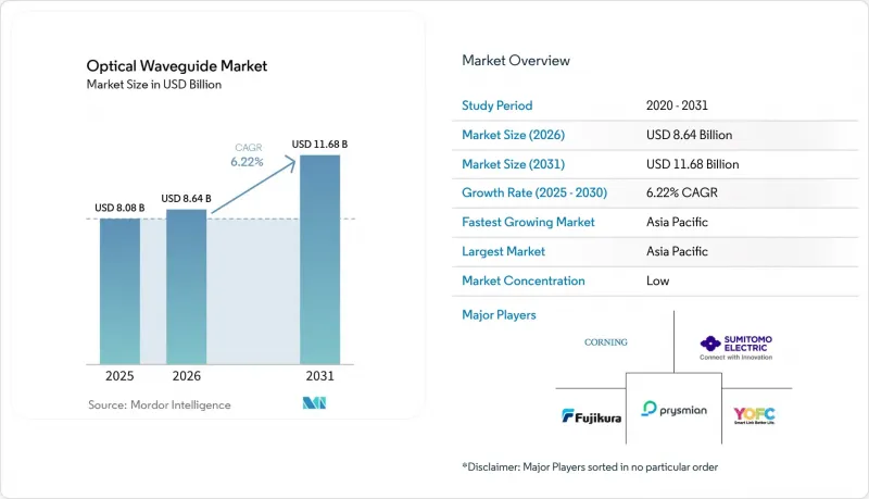
Optical Waveguide - Market Share Analysis, Industry Trends & Statistics, Growth Forecasts (2026 - 2031)
According to Mordor Intelligence, the optical waveguide market size is projected to expand from USD 8.08 billion in 2025 and USD 8.64 billion in 2026 to USD 11.68 billion by 2031, registering a CAGR of 6.22% between 2026 to 2031.
This report is Segmented by Waveguide Type (Planar, Channel/Strip, and More), Material (Glass/Silica, and More), Mode Structure (Single-Mode, and Multi-Mode), Application (Telecommunications and Datacom, Industrial and Environmental Sensing, and More), Fabrication Process (Lithographic Etching, Ultrafast Laser Inscription, and More), and Geography. The Market Forecasts are Provided in Terms of Value (USD).
Global Optical Waveguide Market Trends and Insights
Surge in Silicon-Photonics Datacenter Deployments
Hyperscale operators are shifting from discrete optics to co-packaged architectures that situate silicon-nitride or silicon-rich-oxide waveguides beside 5-nanometer switch cores. Multi-year purchase commitments from tier-one cloud providers now underwrite entire foundry runs, accelerating design cycles and standardizing electro-optical interfaces across switch silicon. Volume production that began in 2026 collapses qualification timelines because the photonics die and ASIC share a single test flow, boosting the optical waveguide market penetration in core switches and line cards. Power envelopes below 5 watts per 1.6 terabit lane make optical links attractive against retimer-heavy electrical backplanes, especially as rack densities move past 30 kilowatts. Combined, these forces elevate attach rates in datacenter capital-expenditure budgets and underpin the most influential demand inflection for the optical waveguide market this decade.
5G and Fiber-to-the-Home Roll-Outs Demanding Low-Loss Integrated Waveguides
Carrier-grade passive optical networks split a single feeder into 32 to 64 drops, mandating planar-lightwave-circuit splitters with sub-0.3 decibel insertion loss. National broadband programs underway across Asia-Pacific, the Middle East, and parts of South America upgrade copper last-mile links to fiber, guaranteeing multi-year volume visibility for low-loss silica and glass waveguides. Equipment vendors integrate waveguide-based wavelength-division multiplexers directly into optical line terminals, shrinking the rack footprint and trimming power draw by eliminating separate splitter trays. Urban build-outs are mirrored by rural subsidies that fund hardened outdoor enclosures where polymer waveguides tolerate extreme temperature swings better than silica, further broadening the materials mix. Deployment velocity keeps factory utilization high and offsets cyclical pauses in datacenter spending, stabilizing baseline growth for the optical waveguide market.
High Capital Intensity of Lithographic Fabs for Sub-Micron Waveguides
Extreme-ultraviolet (193-nanometer) immersion tools cost upward of USD 150 million, and only a dozen global customers operate the latest steppers. Photonic designers therefore compete with higher-margin logic and memory for wafer starts, stretching prototype lead times to months. Shared foundry models help amortize costs but still impose minimum orders that early-stage firms cannot meet, narrowing the supplier base. Nations without semiconductor ecosystems face additional hurdles in securing utilities, cleanroom talent, and equipment import licenses, delaying waveguide capacity expansion. Unless dedicated photonic fabs achieve sustained utilization or lower-cost maskless lithography matures, capital intensity will remain the chief brake on the growth of the optical waveguide market.
Other drivers and restraints analyzed in the detailed report include:
- Rapid Adoption of Polymer Waveguides in Co-Packaged Optics Modules
- Mid-Infrared Sensing Driving Fluoride-Glass Waveguide Demand
- Complex Coupling Losses Versus Optical Fibers
For complete list of drivers and restraints, kindly check the Table Of Contents.
Segment Analysis
Planar designs captured 37.29% of revenue in 2025, anchoring telecom passive components through maturity, low cost, and insertion losses below 0.2 decibels per centimeter. Photonic-crystal implementations, although starting from a small base, are forecast to grow at 7.11% annually as defense contractors embed air-core bandgap structures into compact LiDAR, widening the optical waveguide market addressable sensor field. Channel, fiber, and ridge variants serve optical backplanes and modulators that trade ultra-low loss for tighter bends, while the photonic-crystal class sacrifices fabrication simplicity for unmatched confinement. Together, these form factors illustrate how the optical waveguide market balances legacy volume with frontier performance needs.
Volume advantages accrue to planar silica, where wafer-scale dicing yields thousands of identical splitters that underpin passive optical networks worldwide. Fiber waveguides, although technologically static, remain irreplaceable wherever splice compatibility outweighs integration density. Ridge geometries occupy the performance midpoint and dominate silicon photonics modulators shipped in 400-gigabit and 800-gigabit pluggable transceivers. Photonic-crystal lines are incubated in defense labs and now migrate to commercial drones, spotlighting a premium niche whose influence on the broader optical waveguide market will expand alongside advanced sensing budgets.
Glass and silica platforms held 48.91% of 2025 revenue, underscoring their 30-year incumbency and unrivaled loss floor in passive splitters, an advantage that stabilizes half of the optical waveguide market size. Polymer lines, on a 6.72% CAGR path, benefit from low-temperature deposition that pairs seamlessly with package substrates, enabling faster prototyping and lower capex per layer. Semiconductor materials, silicon, silicon nitride, indium phosphide, and gallium arsenide, provide active modulation, detection, and amplification, prerequisites for co-packaged AI accelerators and coherent telecom links.
Silica's dominance persists in fiber-to-the-home gear, yet data-center silicon-nitride circuits already integrate drivers, photodiodes, and waveguides on one die, cutting board real estate by double digits. Lithium niobate thin films re-enter volume production with CHIPS Act funding, offering electro-optic coefficients an order of magnitude above those of silicon while keeping propagation loss below 0.1 decibel per centimeter. The diverging performance envelopes enable material coexistence and broaden the market's application reach, a duality that enhances the optical waveguide market's resilience against single-material supply disruptions.
Geography Analysis
Asia-Pacific contributed 32.63% of global revenue in 2025 and is expanding at a 7.25% CAGR, the fastest regional pace in the optical waveguide market. China, Japan, and South Korea collectively invest more than USD 21 billion in silicon photonics capacity, funding 300-millimeter fabs that co-package waveguides with memory and logic. National broadband policies extend fiber-to-the-home beyond megacities, securing large passive component orders that lock in fab utilization.
North America remains critical due to CHIPS Act incentives exceeding USD 30 billion and its outsized share of hyperscale data centers. Pilot lines for indium-phosphide and lithium-niobate modulators progress, but construction lead times prolong first-silicon into late 2027, tempering near-term shipment growth. Europe targets a USD 56.5 billion turnover by 2035 under Photonics21, yet fragmented national programs delay the development of unified supply chains, a gap that Asia-Pacific bridges through centrally planned megafabs.
South America scales fiber backbones across Brazil and Argentina, importing planar-lightwave circuits from Asia-Pacific to sidestep local capex. Middle Eastern smart-city ventures such as NEOM specify 10 terabit backbones populated with waveguide-based multiplexers, although project slippage past 2030 blunts immediate impact. Africa's fiber penetration below 5% signals long-term potential but near-term demand headwinds. Overall, regional dynamics preserve Asia-Pacific's lead while keeping multilateral funding momentum intact for the optical waveguide market.
- Corning Incorporated
- Sumitomo Electric Industries, Ltd.
- Fujikura Ltd.
- Prysmian S.p.A.
- Yangtze Optical Fibre and Cable Joint Stock Limited Company
- Teem Photonics SA
- HC Photonics Corporation
- Covesion Ltd.
- Lightwave Logic, Inc.
- Gooch & Housego PLC
- SCHOTT AG
- Coherent Corp.
- Lumentum Holdings Inc.
- NKT Photonics A/S
- Lionix International BV
- Enablence Technologies Inc.
- Accelink Technologies Co., Ltd.
- Hoya Corporation
- Broadcom Inc.
- LightPath Technologies, Inc.
Additional Benefits:
- The market estimate (ME) sheet in Excel format
- 3 months of analyst support
TABLE OF CONTENTS
1 INTRODUCTION
- 1.1 Study Assumptions and Market Definition
- 1.2 Scope of the Study
2 RESEARCH METHODOLOGY
3 EXECUTIVE SUMMARY
4 MARKET LANDSCAPE
- 4.1 Market Overview
- 4.2 Market Drivers
- 4.2.1 Surge in Silicon-Photonics Datacenter Deployments
- 4.2.2 5G/FTTH Roll-Outs Demanding Low-Loss Integrated Waveguides
- 4.2.3 Rapid Adoption of Polymer Waveguides in Co-Packaged Optics Modules
- 4.2.4 Mid-Infrared Sensing Driving Fluoride-Glass Waveguide Demand
- 4.2.5 Defense LiDAR Programs Leveraging Low-SWaP PIC Waveguides
- 4.2.6 Government Chip-On-Board Photonics Funding
- 4.3 Market Restraints
- 4.3.1 Complex Coupling Losses Versus Optical Fibers
- 4.3.2 High Capital Intensity of Lithographic Fabs for Sub-Micron Waveguides
- 4.3.3 Material Thermo-Optic Instability in Extreme Environments
- 4.3.4 IP Bottlenecks Around Proprietary PLC and AWG Designs
- 4.4 Industry Value-Chain Analysis
- 4.5 Regulatory Landscape
- 4.6 Technological Outlook
- 4.7 Impact of Macroeconomic Factors on the Market
- 4.8 Porter's Five Forces Analysis
- 4.8.1 Threat of New Entrants
- 4.8.2 Bargaining Power of Suppliers
- 4.8.3 Bargaining Power of Buyers
- 4.8.4 Threat of Substitutes
- 4.8.5 Competitive Rivalry
5 MARKET SIZE AND GROWTH FORECASTS (VALUE)
- 5.1 By Waveguide Type
- 5.1.1 Planar Waveguides
- 5.1.2 Channel / Strip Waveguides
- 5.1.3 Fiber Waveguides
- 5.1.4 Ridge / Rib Waveguides
- 5.1.5 Photonic-Crystal Waveguides
- 5.2 By Material
- 5.2.1 Glass / Silica
- 5.2.2 Polymer
- 5.2.3 Semiconductor (Si, SiN, InP, GaAs)
- 5.2.4 Lithium-Niobate and Other Crystalline
- 5.3 By Mode Structure
- 5.3.1 Single-Mode
- 5.3.2 Multi-Mode
- 5.4 By Application
- 5.4.1 Telecommunications and Datacom
- 5.4.2 Industrial and Environmental Sensing
- 5.4.3 Medical and Life Sciences
- 5.4.4 Consumer Electronics and AR/VR
- 5.4.5 Defense and Aerospace
- 5.5 By Fabrication Process
- 5.5.1 Lithographic Etching
- 5.5.2 Ultrafast Laser Inscription
- 5.5.3 Ion-Exchange
- 5.5.4 Sol-Gel / CVD
- 5.6 By Geography
- 5.6.1 North America
- 5.6.1.1 United States
- 5.6.1.2 Canada
- 5.6.1.3 Mexico
- 5.6.2 South America
- 5.6.2.1 Brazil
- 5.6.2.2 Argentina
- 5.6.2.3 Rest of South America
- 5.6.3 Europe
- 5.6.3.1 Germany
- 5.6.3.2 United Kingdom
- 5.6.3.3 France
- 5.6.3.4 Russia
- 5.6.3.5 Rest of Europe
- 5.6.4 Asia-Pacific
- 5.6.4.1 China
- 5.6.4.2 Japan
- 5.6.4.3 India
- 5.6.4.4 South Korea
- 5.6.4.5 Australia
- 5.6.4.6 Rest of Asia-Pacific
- 5.6.5 Middle East
- 5.6.5.1 Saudi Arabia
- 5.6.5.2 United Arab Emirates
- 5.6.5.3 Rest of Middle East
- 5.6.6 Africa
- 5.6.6.1 South Africa
- 5.6.6.2 Egypt
- 5.6.6.3 Rest of Africa
- 5.6.1 North America
6 COMPETITIVE LANDSCAPE
- 6.1 Market Concentration
- 6.2 Strategic Moves
- 6.3 Market Share Analysis
- 6.4 Company Profiles (includes Global Level Overview, Market Level Overview, Core Segments, Financials as available, Strategic Information, Market Rank/Share, Products and Services, Recent Developments)
- 6.4.1 Corning Incorporated
- 6.4.2 Sumitomo Electric Industries, Ltd.
- 6.4.3 Fujikura Ltd.
- 6.4.4 Prysmian S.p.A.
- 6.4.5 Yangtze Optical Fibre and Cable Joint Stock Limited Company
- 6.4.6 Teem Photonics SA
- 6.4.7 HC Photonics Corporation
- 6.4.8 Covesion Ltd.
- 6.4.9 Lightwave Logic, Inc.
- 6.4.10 Gooch & Housego PLC
- 6.4.11 SCHOTT AG
- 6.4.12 Coherent Corp.
- 6.4.13 Lumentum Holdings Inc.
- 6.4.14 NKT Photonics A/S
- 6.4.15 Lionix International BV
- 6.4.16 Enablence Technologies Inc.
- 6.4.17 Accelink Technologies Co., Ltd.
- 6.4.18 Hoya Corporation
- 6.4.19 Broadcom Inc.
- 6.4.20 LightPath Technologies, Inc.
7 MARKET OPPORTUNITIES AND FUTURE OUTLOOK
- 7.1 White-Space and Unmet-Need Assessment

