PUBLISHER: Mordor Intelligence | PRODUCT CODE: 2062415

PUBLISHER: Mordor Intelligence | PRODUCT CODE: 2062415
Diffractive Optical Elements - Market Share Analysis, Industry Trends & Statistics, Growth Forecasts (2026 - 2031)
According to Mordor Intelligence, the diffractive optical elements market was USD 305.43 million in 2025 and USD 334.17 million in 2026, and is forecast to reach USD 523.91 million by 2031, growing at a CAGR of 9.41% from 2026 to 2031.
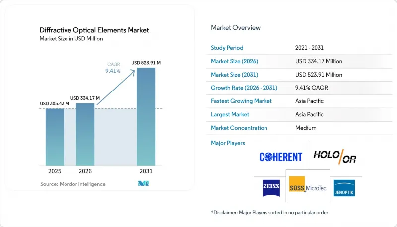
This report is Segmented by Product Type (Beam Shapers, Beam Splitters, and More), Material (Fused Silica and Quartz, and More), Fabrication Technology (Photolithography and Reactive-Ion Etching, and More), Application (Laser Material Processing, and More), End-User Industry (Industrial Manufacturing, Healthcare, and More), and Geography. The Market Forecasts are Provided in Terms of Value (USD).
Global Diffractive Optical Elements Market Trends and Insights
Rising Adoption Of Beam-Shaping DOEs In High-Power Fiber Lasers
In the diffractive optical elements market, industrial welding, cutting, and additive manufacturing require uniform irradiance profiles that refractive optics cannot maintain at multi-kilowatt power levels. Recent nanoimprint-fabricated elements combine beam shaping and splitting in a single wafer, cutting part count and thermal lensing risks. Thin fused-silica substrates maintain high damage thresholds and minimal dispersion for femtosecond pulses, while off-the-shelf availability has trimmed traditional 8-12 week lead times to a matter of days, accelerating system-integrator deployment.Industrial laser lines for battery welding, sheet cutting, and turbine drilling require uniform irradiance that conventional refractive optics cannot deliver at kilowatt levels, so integrators now specify fused-silica diffractive beam shapers that withstand >10 J cm-2 fluence with negligible dispersion.
Cost Reduction Pressure Accelerating Injection-Molded Polymer DOEs
Injection molding and nanoimprint replication reduce unit cost by roughly one order of magnitude versus etched fused silica. In 2026, a smartphone platform integrated nanopillar metasurfaces, achieving a 73% cost reduction and paving the way for mass-market 3-D sensing.Metalenz licensed its metasurface IP to STMicroelectronics, and more than 140 million polymer metasurface units shipped by mid-2025, confirming the yield scalability of wafer-level replication. VIAOPTIC studies show that polymethyl methacrylate delivers high optical purity, while polycarbonate withstands 145 °C cabin peaks, so handset and automotive Tier-1s match polymers to use cases.
High Precision Fabrication Cost for Sub-Micron Features
In the diffractive optical elements market, photolithography combined with reactive-ion etching delivers +-5-nanometer depth control, yet throughput remains near 15 cm2 per hour on 150-millimeter wafers, pushing custom DOE prices above USD 500 per piece. Grayscale-lithography shortcuts can lower cost but are limited to binary or four-level phase structures, which restricts advanced wavefront engineering. The resulting bifurcation places nanoimprint lines in consumer electronics and direct-write shops in aerospace, leaving mid-volume tooling underserved.
Other drivers and restraints analyzed in the detailed report include:
- Surge in Automotive LiDAR Programs Integrating Meta-Surface DOEs
- Increased Deployment Of Three-Dimensional Sensing Cameras In Smartphones
- Limited Thermal Stability of Polymer DOEs in Harsh Environments
For complete list of drivers and restraints, kindly check the Table Of Contents.
Segment Analysis
Beam shapers captured 42.52% of 2025 revenue, reflecting their role in battery-pack welding, turbine-blade drilling, and sheet-metal cutting lines where top-hat profiles prevent edge burn-through. Diffractive diffusers also support fractional dermatology lasers cleared by the U.S. FDA, enabling uniform micro-spot arrays that quicken patient recovery. The diffractive optical elements market for beam shapers is expected to continue expanding as industrial OEMs prequalify off-the-shelf diffusers to shorten design cycles.
Vortex phase plates and axicons are projected to grow at an 11.42% CAGR through 2031, as quantum research teams exploit orbital-angular-momentum beams for information encoding. Demonstrations of spiral zone plates with 40% first-order efficiency point toward optical trapping and free-space communication payloads. Although unit volumes remain modest, the diffractive optical elements market share held by vortex products is poised to expand as chip-scale phase-modulated lasers enter commercial quantum sensors.
Fused-silica and quartz supplied 51.85% of 2025 material revenue thanks to low thermal expansion below 0.5 ppm/K and UV-to-IR transmission that meets semiconductor lithography and high-energy laser demands. Global capacity, however, is constrained by parts-per-billion impurity specifications that only a handful of suppliers achieve, prolonging lead times for next-generation EUV optics. The diffractive optical elements market size tied to fused-silica products, therefore, commands a pricing premium that buffers suppliers against commodity pressures.
Diamond substrates are forecast to clock a 12.21% CAGR on the back of defense laser splitters requiring thermal conductivity near 2000 W/m-K. SBIR awards in the United States have enabled small-batch production of 300-kilowatt continuous-wave systems, validating technical feasibility even as wafer costs exceed USD 5,000 per 100-millimeter wafer. Once deposition yields improve, diamond could erode fused silica's market share in diffractive optical elements for weapon-class applications.
Geography Analysis
Asia-Pacific generated 40.32% of 2025 revenue and is on track for a 12.89% CAGR through 2031. Wafer-scale metasurface projects in Tianjin and roll-to-roll metalens printing breakthroughs in South Korea point to dominant regional capacity, while Japanese optoelectronics firms commercialize phase-modulated laser arrays that collapse module footprints. Local governments continue to subsidize 12-inch wafer fabs that will push the diffractive optical elements market deeper into consumer electronics and automotive perception modules.
North America benefits from defense funding and the expansion of cloud data centers. A USD 2 billion equity investment tied to AI optical interconnects underscores a strategic commitment to wafer-level DOE fabrication. Concurrent SBIR awards target 300-kilowatt naval laser splitters, aligning with diamond-substrate development timelines. The region, therefore, balances high-mix aerospace orders with volume silicon photonics programs, diversifying its share of the diffractive optical elements market.
Europe sustains momentum through automotive LiDAR integration and semiconductor lithography optics. Clean-room expansions in Germany will add EUV and high-NA immersion capacity by 2027, while regional carmakers specify metasurface beam shapers to meet Euro NCAP safety targets. South America, the Middle East and Africa remain nascent, but solar-panel texturing and oil-field inspection create niche demand for rugged fused-silica DOEs in high-temperature and high-dust conditions.
- Jenoptik AG
- HOLO/OR Ltd.
- Holographix LLC
- Santec Corporation
- Edmund Optics Inc.
- Altechna UAB
- LightTrans International UG
- SILIOS Technologies SA
- Hamamatsu Photonics K.K.
- Coherent Corp.
- Meta Materials Inc.
- Luminit LLC
- Panasonic Holdings Corporation
- Samsung Electronics Co., Ltd.
- Microsoft Corporation
- LG Electronics Inc.
- Fujifilm Corporation
- Holochip Corporation
- Photon Design Ltd.
- Pioneer Photonics
Additional Benefits:
- The market estimate (ME) sheet in Excel format
- 3 months of analyst support
TABLE OF CONTENTS
1 INTRODUCTION
- 1.1 Study Assumptions and Market Definition
- 1.2 Scope of the Study
2 RESEARCH METHODOLOGY
3 EXECUTIVE SUMMARY
4 MARKET LANDSCAPE
- 4.1 Market Overview
- 4.2 Market Drivers
- 4.2.1 Rising Adoption of Beam-Shaping DOEs in High-Power Fiber Lasers
- 4.2.2 Cost Reduction Pressure Accelerating Injection-Molded Polymer DOEs
- 4.2.3 Surge in Automotive LiDAR Programs Integrating Meta-Surface DOEs
- 4.2.4 Emerging Quantum Photonics Applications Requiring Complex Phase Plates
- 4.2.5 Increased Deployment of 3-D Sensing Cameras in Smartphones
- 4.2.6 Defense Investments in High-Energy Laser Weapon Beam Splitters
- 4.3 Market Restraints
- 4.3.1 High Precision Fabrication Cost for Sub-Micron Features
- 4.3.2 Limited Thermal Stability of Polymer DOEs in Harsh Environments
- 4.3.3 Supply Chain Bottlenecks for Ultrapure Fused Silica Blanks
- 4.3.4 IP Fragmentation Hindering Standardization Across Suppliers
- 4.4 Industry Value Chain Analysis
- 4.5 Regulatory Landscape
- 4.6 Technological Outlook
- 4.7 Impact of Macroeconomic Factors
- 4.8 Porter's Five Forces Analysis
- 4.8.1 Bargaining Power of Suppliers
- 4.8.2 Bargaining Power of Buyers
- 4.8.3 Threat of New Entrants
- 4.8.4 Threat of Substitutes
- 4.8.5 Intensity of Competitive Rivalry
5 MARKET SIZE AND GROWTH FORECASTS
- 5.1 By Product Type
- 5.1.1 Beam Shapers
- 5.1.2 Diffusers/Homogenizers
- 5.1.3 Beam Splitters
- 5.1.4 Vortex Phase Plates and Axicons
- 5.2 By Material
- 5.2.1 Fused Silica and Quartz
- 5.2.2 Polymers (PMMA, Polycarbonate, Zeonex)
- 5.2.3 Silicon and Silicon Nitride
- 5.2.4 Diamond
- 5.3 By Fabrication Technology
- 5.3.1 Photolithography and Reactive-Ion Etching
- 5.3.2 Direct Laser Writing
- 5.3.3 Electron-Beam Lithography
- 5.3.4 Nano-Imprint / Injection Molding
- 5.4 By Application
- 5.4.1 Laser Material Processing
- 5.4.2 Medical and Aesthetic Procedures
- 5.4.3 3-D Sensing and LiDAR
- 5.4.4 Optical Communications and Free-Space Optics
- 5.4.5 AR/VR and Holographic Displays
- 5.5 By End-User Industry
- 5.5.1 Industrial Manufacturing
- 5.5.2 Healthcare
- 5.5.3 Consumer Electronics
- 5.5.4 Automotive and Transportation
- 5.5.5 Aerospace and Defense
- 5.6 By Geography
- 5.6.1 North America
- 5.6.1.1 United States
- 5.6.1.2 Canada
- 5.6.1.3 Mexico
- 5.6.2 South America
- 5.6.2.1 Brazil
- 5.6.2.2 Argentina
- 5.6.2.3 Rest of South America
- 5.6.3 Europe
- 5.6.3.1 Germany
- 5.6.3.2 France
- 5.6.3.3 United Kingdom
- 5.6.3.4 Italy
- 5.6.3.5 Rest of Europe
- 5.6.4 Asia-Pacific
- 5.6.4.1 China
- 5.6.4.2 Japan
- 5.6.4.3 South Korea
- 5.6.4.4 India
- 5.6.4.5 Rest of Asia-Pacific
- 5.6.5 Middle East and Africa
- 5.6.1 North America
6 COMPETITIVE LANDSCAPE
- 6.1 Market Concentration
- 6.2 Strategic Moves
- 6.3 Market Share Analysis
- 6.4 Company Profiles (includes Global Level Overview, Market Level Overview, Core Segments, Financials as available, Strategic Information, Market Rank/Share, Products and Services, Recent Developments)
- 6.4.1 Jenoptik AG
- 6.4.2 HOLO/OR Ltd.
- 6.4.3 Holographix LLC
- 6.4.4 Santec Corporation
- 6.4.5 Edmund Optics Inc.
- 6.4.6 Altechna UAB
- 6.4.7 LightTrans International UG
- 6.4.8 SILIOS Technologies SA
- 6.4.9 Hamamatsu Photonics K.K.
- 6.4.10 Coherent Corp.
- 6.4.11 Meta Materials Inc.
- 6.4.12 Luminit LLC
- 6.4.13 Panasonic Holdings Corporation
- 6.4.14 Samsung Electronics Co., Ltd.
- 6.4.15 Microsoft Corporation
- 6.4.16 LG Electronics Inc.
- 6.4.17 Fujifilm Corporation
- 6.4.18 Holochip Corporation
- 6.4.19 Photon Design Ltd.
- 6.4.20 Pioneer Photonics
7 MARKET OPPORTUNITIES AND FUTURE OUTLOOK
- 7.1 White-Space and Unmet-Need Assessment

