PUBLISHER: Mordor Intelligence | PRODUCT CODE: 2064402

PUBLISHER: Mordor Intelligence | PRODUCT CODE: 2064402
GPU-Grade Silicon Wafer - Market Share Analysis, Industry Trends & Statistics, Growth Forecasts (2026 - 2031)
According to Mordor Intelligence, the gPU-grade silicon wafer market size is expected to expand from USD 4.31 billion in 2025 to USD 4.80 billion in 2026 and reach USD 7.39 billion by 2031, growing at an 18.85% CAGR from 2026 to 2031.
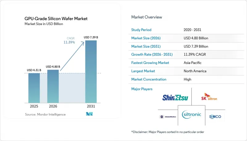
This report is Segmented by Wafer Type (Polished Prime Wafers, Epitaxial Wafers, and SOI Wafers), Process Node (Leading Edge Nodes Below 7 Nm, and Advanced Nodes 7-14 Nm), End Customer Type (Pure-Play Foundries, and IDMs), and Geography (North America, Europe, Asia-Pacific, and Rest of the World). Market Forecasts are Provided in Terms of Value (USD).
Global GPU-Grade Silicon Wafer Market Trends and Insights
Exploding AI Training Compute Density Driving Ultra-Low Defect Requirements
GPU clusters now exceed 100,000 accelerators per installation, so a single wafer defect can cascade into millions of dollars in lost revenue. TSMC's 3 nm N3E node requires defect densities below 0.09 defects/cm2 to sustain yields above 70%. Shin-Etsu and SUMCO have therefore integrated advanced inline metrology that reduces scrap by 15% to 20% while polishing surface micro-roughness to sub-0.1 nm levels. Tighter specifications prolong qualification cycles to as much as 9 months, but they also raise switching costs and reinforce supplier stickiness with the leading foundries.
Rapid Ramp of 3 nm and 2 nm GPU Architectures Increasing 300 mm Prime Wafer Demand
TSMC devoted about 40% of its 300 mm capacity to sub-5 nm nodes in 2025, equating to roughly 1.2 million wafer starts per month, while Samsung Foundry targets 50,000 wafer starts per month on its 3 nm gate-all-around line by late 2026. Node shrinkage, enlarged reticle sizes, and drive a 20%-30% uplift in wafer consumption per finished die. SUMCO responded by boosting its Japanese epi capacity 15% in 2025 to keep pace with AI accelerators. The jump to 2 nm in 2027-2028 will further tighten flatness and purity requirements, entrenching premium pricing for prime substrates.
Limited High-Purity Polysilicon Supply Constraining 300 mm Output
Only Hemlock Semiconductor, Wacker Chemie, and OCI consistently achieve 11-nines purity, and combined semiconductor-grade output of roughly 180,000 t yr-1 in 2025 fell short of the 200,000 t yr-1 required for wafers and solar cells. Lead times for new orders stretched to 40 weeks at Wacker's Burghausen facility, prompting wafer vendors to ration allocations toward long-term contracts. Hemlock's USD 250 million Tennessee expansion will add 10,000 t yr-1 by 2027, but barely covers incremental demand from U.S. CHIPS Act fabs.
Other drivers and restraints analyzed in the detailed report include:
- Shift Toward Backside Power Delivery Necessitating Thicker Epi Wafer Specs
- Localization Incentives in U.S. and Europe for Strategic Wafer Supply
- Long Qualification Cycles with GPU Customers Slowing Node Transitions
For complete list of drivers and restraints, kindly check the Table Of Contents.
Segment Analysis
Epitaxial substrates are experiencing the fastest growth, with a CAGR of 11.99% projected through 2031. This growth is driven by the increasing demand for backside power delivery and through-silicon vias, which require 10-15 µm epi thicknesses that polished prime wafers cannot support. In 2025, polished prime wafers accounted for 57% of revenue, ensuring the GPU-grade silicon wafer market for mainstream nodes remains significant. However, this dominance is expected to decline as nodes of 3 nm and below enter mass production. Intel's PowerVia roadmap highlights this transition, with its 18A designs relying heavily on epitaxial surfaces capable of handling aggressive via aspect ratios.
The market share of SOI substrates within the GPU-grade silicon wafer market, although relatively small in 2025, is steadily increasing. This growth is attributed to the reliance of chiplet layouts on low-capacitance interposers. Soitec's Smart Cut technology plays a pivotal role in this trend by depositing a 20 nm buried oxide layer beneath a 6 nm active layer, facilitating heterogeneous stacking while reducing thermal resistance. Despite cost pressures making polished prime wafers more appealing for nodes of 7 nm and above, the superior yields and power efficiency at the leading edge continue to drive investments in epitaxial substrates.
Geography Analysis
Asia-Pacific controlled 68% of 2025 revenue thanks to TSMC's Hsinchu and Tainan megafabs alongside Samsung's Hwaseong and Pyeongtaek complexes, which together ran about 2.5 million 300 mm wafers per month for leading-edge GPUs. Japan and South Korea, home to Shin-Etsu, SUMCO, and SK Siltron, supplied roughly 55% of global substrate output, underscoring the region's depth across the value chain. China accounted for 12%-15% of consumption but faces an effective ceiling after December 2024, when export controls blocked ASML deep-ultraviolet tools, capping domestic 7 nm capability.
North America is the fastest-growing region, with a 11.79% CAGR through 2031. CHIPS Act grants of USD 52.7 billion, led by the USD 400 million award to GlobalWafers, will add 1.2 million wafers per year in Texas from 2028. Intel's Foundry Services expansions in Arizona, New Mexico, and Ohio, plus hyperscaler demand for sovereign AI capacity, funnel steady offtake into domestic plants. The GPU-grade silicon wafer market in North America could double by 2031 if scheduled fabs come online as planned.
Europe captured 8% of 2025 revenue, clustered in Germany's Saxony region where Infineon, Bosch, and GlobalFoundries operate mature-node lines. Siltronic's EUR 3.5 billion (USD 3.85 billion) Dresden investment, underwritten by EUR 1.2 billion (USD 1.32 billion) in EU Chips Act grants, is set to lift the continent's share to roughly 12%-14% by 2031. Middle East and Africa together with South America remain minor, at under 2% combined, while India's incentive program has yet to translate into shovel-ready wafer projects.
- Shin-Etsu Handotai Co., Ltd.
- SUMCO Corporation
- Siltronic AG
- GlobalWafers Co., Ltd.
- SK Siltron Co., Ltd.
- Wafer Works Corp.
- Soitec S.A.
- Shanghai Simgui Technology Co., Ltd.
- Okmetic Oyj
- Ferrotec Holdings Corporation
- Hangzhou Silicon Tech Co., Ltd. (HJSemi)
- Zhonghuan Semiconductor Co., Ltd.
- POSCO Future M Co., Ltd.
- Episil-Precision Inc.
- MEMC Korea Company
- Korea Silicon Wafer Co., Ltd.
- Linton Crystal Technologies
- Salem Advanced Materials Inc.
- Noel Technologies
- Topsil GlobalWafers
Additional Benefits:
- The market estimate (ME) sheet in Excel format
- 3 months of analyst support
TABLE OF CONTENTS
1 INTRODUCTION
- 1.1 Study Assumptions and Market Definition
- 1.2 Scope of the Study
2 RESEARCH METHODOLOGY
3 EXECUTIVE SUMMARY
4 MARKET LANDSCAPE
- 4.1 Market Overview
- 4.2 Market Drivers
- 4.2.1 Exploding AI Training Compute Density Driving Ultra-Low Defect Requirements
- 4.2.2 Rapid Ramp of 3 nm and 2 nm GPU Architectures Increasing 300 mm Prime Wafer Demand
- 4.2.3 Shift Toward Backside Power Delivery Necessitating Thicker Epi Wafer Specs
- 4.2.4 Localization Incentives in U.S. and Europe for Strategic Wafer Supply
- 4.2.5 Emergence of Chiplet-Based GPU Designs Boosting Demand for Large-Area SOI Wafers
- 4.2.6 Sustainability Mandates Driving Adoption of Reclaimed Prime Wafers for R&D
- 4.3 Market Restraints
- 4.3.1 Limited High-Purity Polysilicon Supply Constraining 300 mm Output
- 4.3.2 Long Qualification Cycles with GPU Customers Slowing Node Transitions
- 4.3.3 Capital Intensity of Float-Zone 300 mm Lines Deterring New Entrants
- 4.3.4 Trade Restrictions on Advanced Node Equipment Limiting Expansion in China
- 4.4 Impact of Macroeconomic Factors on the Market
- 4.5 Industry Value Chain Analysis
- 4.6 Regulatory Landscape
- 4.7 Technological Outlook
- 4.8 Porter's Five Forces Analysis
- 4.8.1 Bargaining Power of Suppliers
- 4.8.2 Bargaining Power of Buyers
- 4.8.3 Threat of New Entrants
- 4.8.4 Threat of Substitutes
- 4.8.5 Intensity of Competitive Rivalry
5 MARKET SIZE AND GROWTH FORECASTS (VALUE)
- 5.1 By Wafer Type
- 5.1.1 Polished Prime Wafers
- 5.1.2 Epitaxial (Epi) Wafers
- 5.1.3 SOI (Silicon-on-Insulator) Wafers
- 5.2 By Process Node
- 5.2.1 Leading Edge Nodes (<7 nm)
- 5.2.2 Advanced Nodes (7-14 nm)
- 5.3 By End Customer Type
- 5.3.1 Pure-Play Foundries
- 5.3.2 Integrated Device Manufacturers (IDMs)
- 5.4 By Geography
- 5.4.1 North America
- 5.4.1.1 United States
- 5.4.1.2 Canada
- 5.4.1.3 Mexico
- 5.4.2 Europe
- 5.4.2.1 United Kingdom
- 5.4.2.2 Germany
- 5.4.2.3 Rest of Europe
- 5.4.3 Asia-Pacific
- 5.4.3.1 China
- 5.4.3.2 Japan
- 5.4.3.3 India
- 5.4.3.4 South Korea
- 5.4.3.5 Rest of Asia-Pacific
- 5.4.4 Rest of the World
- 5.4.1 North America
6 COMPETITIVE LANDSCAPE
- 6.1 Market Concentration
- 6.2 Strategic Moves
- 6.3 Market Share Analysis
- 6.4 Company Profiles (includes Global Level Overview, Market Level Overview, Core Segments, Financials as available, Strategic Information, Market Rank/Share, Products and Services, Recent Developments)
- 6.4.1 Shin-Etsu Handotai Co., Ltd.
- 6.4.2 SUMCO Corporation
- 6.4.3 Siltronic AG
- 6.4.4 GlobalWafers Co., Ltd.
- 6.4.5 SK Siltron Co., Ltd.
- 6.4.6 Wafer Works Corp.
- 6.4.7 Soitec S.A.
- 6.4.8 Shanghai Simgui Technology Co., Ltd.
- 6.4.9 Okmetic Oyj
- 6.4.10 Ferrotec Holdings Corporation
- 6.4.11 Hangzhou Silicon Tech Co., Ltd. (HJSemi)
- 6.4.12 Zhonghuan Semiconductor Co., Ltd.
- 6.4.13 POSCO Future M Co., Ltd.
- 6.4.14 Episil-Precision Inc.
- 6.4.15 MEMC Korea Company
- 6.4.16 Korea Silicon Wafer Co., Ltd.
- 6.4.17 Linton Crystal Technologies
- 6.4.18 Salem Advanced Materials Inc.
- 6.4.19 Noel Technologies
- 6.4.20 Topsil GlobalWafers
7 MARKET OPPORTUNITIES AND FUTURE OUTLOOK
- 7.1 White-Space and Unmet-Need Assessment

