PUBLISHER: Mordor Intelligence | PRODUCT CODE: 2098541

PUBLISHER: Mordor Intelligence | PRODUCT CODE: 2098541
AI Accelerator Memory - Market Share Analysis, Industry Trends & Statistics, Growth Forecasts (2026 - 2031)
According to Mordor Intelligence, the AI accelerator memory market size is expected to grow from USD 38.29 billion in 2025 to USD 53.74 billion in 2026 and is forecast to reach USD 165.79 billion by 2031 at 25.27% CAGR over 2026-2031.
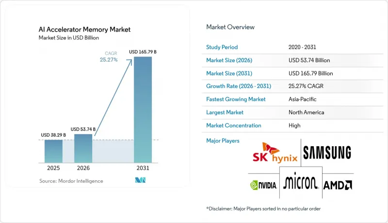
This report is Segmented by Memory Architecture (HBM, and More), Accelerator Platform (Data Center GPU Accelerators, and More), HBM Generation (HBM2 and HBM2E, and More), HBM Stack Height (Up To 4-High, and More), HBM Capacity Per Stack (Up To 8 GB, and More), Deployment Platform (Hyperscale Cloud and AI Factories, and More), and Geography. The Market Forecasts are Provided in Terms of Value (USD).
Global AI Accelerator Memory Market Trends and Insights
Growing Adoption of HBM3E and HBM4 in AI Accelerators
The AI accelerator memory market is benefiting from each HBM generation upgrade because higher performance now comes with greater process complexity and higher selling prices. SK hynix stated that its HBM3E reached up to 9.6 Gbps per pin and more than 1.23 TB/s of bandwidth, underscoring why current AI accelerators continue to move toward denser, faster memory configurations. Samsung said in February 2026 that it had begun mass production of HBM4 using a 1c DRAM process and a 4 nm logic base die, signaling that the market had already begun shifting to the next qualification cycle. NVIDIA confirmed in June 2026 that Samsung, SK hynix, and Micron had all qualified and entered production for its Vera Rubin platform, reducing uncertainty around vendor readiness and widening the supply base for the next accelerator ramp. The AI accelerator memory market, therefore, moves higher not only because unit demand is rising, but also because each transition to HBM4 and HBM4E ties revenue growth to a more demanding and more expensive manufacturing path.
Rising AI Training and Inference Compute Density
The AI accelerator memory market is also being pushed by the steady rise in memory capacity and bandwidth required per chip for both training and inference. Google introduced TPU 8i in April 2026 with 288 GB of HBM and 8,601 GB/s per chip, while also tripling on-chip SRAM to 384 MB, demonstrating how memory intensity has risen in one product cycle. NVIDIA's Vera Rubin platform extended that direction with a 576 GB HBM4 configuration per accelerator, indicating that long-context models and larger working sets are still pushing minimum memory requirements upward. JEDEC's LPDDR6 roadmap also showed that even edge systems are moving toward richer memory functions, including processing-in-memory support, which reflects broader pressure to reduce data movement and improve local inference efficiency. In the AI accelerator memory market, this means memory content per accelerator is rising even when model efficiency improves, because longer context windows and more complex inference pipelines continue to consume additional bandwidth and capacity.
High Package-Level Thermal and Yield Constraints
The AI accelerator memory market faces a significant technical constraint; thermal management becomes more difficult as layer counts rise and logic dies are integrated into the base structure. Samsung's HBM4 ramp and the industry's move to higher stack heights show that memory vendors are trying to increase density while staying within qualification and reliability limits. JEDEC standards remain important because commercialization depends on meeting defined thermal and performance thresholds across successive generations. Micron and Marvell both highlighted memory architecture changes aimed at reducing data movement and interface power, confirming that the issue is not limited to raw supply volume but extends to package-level feasibility. This keeps the artificial intelligence (AI) accelerator memory market vulnerable to slower-than-expected ramps whenever new stack heights or new logic-process combinations push yields below commercial targets.
Other drivers and restraints analyzed in the detailed report include:
- Expansion of Hyperscale Data Center AI Fleets
- Higher Bandwidth Demand Per Watt in Advanced GPUs and ASICs
- Limited Qualified Supply Base for Advanced HBM
For complete list of drivers and restraints, kindly check the Table Of Contents.
Segment Analysis
HBM held 92.48% of the AI accelerator memory market share by memory architecture in 2025, which confirms that leading AI accelerators still depend on very high bandwidth and dense on-package memory. Google's Ironwood TPU deployed 8 stacks of HBM3E at 7,370 GB/s per chip, and the later TPU 8i lifted performance to 8,601 GB/s with 288 GB per chip, which shows why HBM stayed the default design choice for frontier systems. GDDR kept a role in lower-cost inference GPUs and workstation cards, where system designers still balance performance against integration cost. DDR also remained relevant for CPU-attached functions in hybrid AI servers, especially when accelerators are deployed alongside broader enterprise compute infrastructure. In the AI accelerator memory market, this wide gap between HBM and the rest of the architecture mix reflects how strongly current data center AI depends on bandwidth-intensive accelerator packages.
LPDDR is the fastest-growing sub-segment, with a 26.27% CAGR from 2026 to 2031, indicating that the next wave of demand is broadening beyond the largest data center deployments. JEDEC said its LPDDR6 roadmap adds processing-in-memory support and extends LPDDR into data centers and edge use cases, suggesting a wider role for low-power memory in AI systems that need local inference and lower energy draw. Samsung's LPDDR6 program targets AI edge systems, AI PCs, data centers, and automotive platforms, confirming that suppliers are treating LPDDR as an AI memory growth area rather than just a mobile component. Micron also linked LPDDR bandwidth directly to token-generation speed in edge AI, making memory throughput a direct performance lever outside the hyperscale cloud. The AI accelerator memory market is therefore splitting into a data center HBM core and a fast-growing edge LPDDR layer, with each architecture serving a distinct deployment model.
Data Center GPU Accelerators captured 73.58% of the AI accelerator memory market size in 2025, reflecting the installed base and allocation strength of mainstream training and inference GPU platforms. NVIDIA's H100, H200, and Blackwell families kept GPU platforms at the center of large-scale AI deployments, while AMD remained a meaningful secondary customer route for HBM supply through platforms such as MI455X in the next cycle. AI SoCs, NPUs, and APUs continued to serve mobile, automotive, and embedded AI, but their memory value per unit remained lower than that of large data center accelerators. FPGA-based accelerators still mattered in latency-sensitive workloads where adaptability and deterministic response times remained important. This left the AI accelerator memory market anchored by GPU-led infrastructure, even as other platform types widened the demand base.
Custom AI ASICs and XPUs are projected to grow at 26.46% CAGR through 2031, making them the fastest-growing platform segment in the AI accelerator memory market. Broadcom said in February 2026 that it began shipping the first 2 nm custom compute SoC on its 3.5D XDSiP architecture, with support for multiple HBM stacks, demonstrating how custom silicon is moving into advanced heterogeneous packaging earlier and faster. AWS Trainium, Google TPU 8, and Meta MTIA 500 indicate that hyperscalers are increasingly designing their memory needs around workload-specific bandwidth and latency targets rather than accepting a standard GPU template. Marvell's custom HBM compute architecture also supports more HBM stacks per XPU with lower interface power, which makes tailored memory interfaces a competitive design feature for custom accelerators. As that shift continues, the AI accelerator memory market will see a broader mix of qualification paths and product-specific HBM configurations than it did in the prior GPU-dominated cycle.
Complete Report Scope:
- By Memory Architecture
- High Bandwidth Memory (HBM)
- Graphics Double Data Rate Memory
- Low-Power Double Data Rate Memory
- Double Data Rate Memory
- Other Specialized Accelerator Memory
- By Accelerator Platform
- Data Center GPU Accelerators
- Custom AI ASICs and XPUs
- AI SoCs, NPUs, and APUs
- FPGA-Based Accelerators
- Data Processing Units, SmartNICs, and Networking Accelerators
- Other Accelerator Platforms
- By HBM Generation
- HBM2 and HBM2E
- HBM3
- HBM3E
- HBM4
- HBM4E and Next-Generation HBM
- By HBM Stack Height
- Up to 4-High
- 8-High
- 12-High
- 16-High
- Above 16-High
- By HBM Capacity per Stack
- Up to 8 GB
- 8 GB to 16 GB
- 16 GB to 24 GB
- 24 GB to 36 GB
- Above 36 GB
- By Deployment Platform
- Hyperscale Cloud and AI Factories
- Enterprise and On-Premise Data Centers
- High-Performance Computing and Research Systems
- Networking and Telecommunications Infrastructure
- Edge AI and Industrial Systems
- AI Workstations and AI PCs
- Automotive AI and Autonomous Systems
- By Geography
- North America
- United States
- Canada
- Mexico
- Europe
- Germany
- United Kingdom
- France
- Italy
- Rest of Europe
- Asia-Pacific
- China
- Japan
- South Korea
- India
- Southeast Asia
- Rest of Asia-Pacific
- South America
- Middle East and Africa
- North America
Geography Analysis
North America held 48.12% of the AI accelerator memory market in 2025, maintaining its position as the leading regional demand center. The region's lead came from the concentration of hyperscale buyers, custom silicon programs, and large AI server deployments rather than from memory manufacturing capacity alone. Amazon's February 2026 decision to invest USD 12 billion in Louisiana showed the scale of single-project commitments that continue to shape regional hardware demand. Google also expanded its TPU roadmap in 2026, reinforcing North America's role as the primary early-deployment zone for memory-intensive accelerators. Canada supported regional growth through favorable power conditions for data centers, while Mexico gained attention as a nearshore infrastructure corridor for future AI buildouts.
Asia-Pacific is projected to grow at 26.19% CAGR through 2031, making it the fastest-growing region in the AI accelerator memory market. The region plays a dual role as both the manufacturing base for advanced HBM and a rising center of demand for AI infrastructure. South Korea remained central through the fab networks of SK hynix and Samsung, while Micron's Hiroshima site added an important production node in the broader Pacific supply chain. SK hynix's KRW 21.61 trillion (approximately USD 16 billion) Yongin cluster approval in February 2026 showed how heavily the region is investing in future memory output. Japan contributed advanced packaging capabilities, and India and Southeast Asia continued to build demand through AI cloud expansion, AI PC adoption, and local inference deployments.
Europe, South America, the Middle East, and Africa remained smaller in current share, but each added strategic demand for the artificial intelligence (AI) accelerator memory market. Germany and the United Kingdom led European AI server deployments, while public initiatives such as France 2030 continued supporting domestic compute capacity. The EU AI Act also encouraged more local infrastructure planning because compliance and data control now influence where enterprise AI workloads are hosted. The Middle East and Africa gained importance through sovereign AI cluster procurement in Saudi Arabia and the UAE, supported by export frameworks and cross-border technology agreements. South America remained earlier in its cycle, but Brazil and Chile continued laying the groundwork for future regional AI infrastructure expansion.
- SK hynix Inc.
- Samsung Electronics Co., Ltd.
- Micron Technology, Inc.
- NVIDIA Corporation
- Advanced Micro Devices, Inc.
- Intel Corporation
- Taiwan Semiconductor Manufacturing Company Limited
- ASML Holding N.V.
- Applied Materials, Inc.
- Lam Research Corporation
- KLA Corporation
- Tokyo Electron Limited
- Amkor Technology, Inc.
- ASE Technology Holding Co., Ltd.
- JCET Group Co., Ltd.
- Powertech Technology Inc.
- Tongfu Microelectronics Co., Ltd.
- Marvell Technology, Inc.
- Synopsys, Inc.
- Cadence Design Systems, Inc.
Additional Benefits:
- The market estimate (ME) sheet in Excel format
- 3 months of analyst support
TABLE OF CONTENTS
1 INTRODUCTION
- 1.1 Study Assumptions and Market Definition
- 1.2 Scope of the Study
2 RESEARCH METHODOLOGY
3 EXECUTIVE SUMMARY
4 MARKET LANDSCAPE
- 4.1 Market Overview
- 4.2 Market Drivers
- 4.2.1 Growing Adoption of HBM3E and HBM4 in AI Accelerators
- 4.2.2 Rising AI Training and Inference Compute Density
- 4.2.3 Expansion of Hyperscale Data Center AI Fleets
- 4.2.4 Higher Bandwidth Demand per Watt in Advanced GPUs and ASICs
- 4.2.5 Supply Reallocation Toward High-Margin AI Memory SKUs
- 4.2.6 Rising Adoption of Chiplet-Based AI Architectures
- 4.3 Market Restraints
- 4.3.1 High Package-Level Thermal and Yield Constraints
- 4.3.2 Limited Qualified Supply Base for Advanced HBM
- 4.3.3 Heavy Dependence on Advanced Packaging Capacity
- 4.3.4 Export Controls and Supply Chain Localization Friction
- 4.4 Industry Value Chain Analysis
- 4.5 Regulatory Landscape
- 4.6 Technological Outlook
- 4.7 Impact of Macroeconomic Factors on the Market
- 4.8 Porter's Five Forces Analysis
- 4.8.1 Bargaining Power of Suppliers
- 4.8.2 Bargaining Power of Buyers
- 4.8.3 Threat of New Entrants
- 4.8.4 Threat of Substitutes
- 4.8.5 Intensity of Competitive Rivalry
5 MARKET SIZE AND GROWTH FORECASTS (VALUE)
- 5.1 By Memory Architecture
- 5.1.1 High Bandwidth Memory (HBM)
- 5.1.2 Graphics Double Data Rate Memory
- 5.1.3 Low-Power Double Data Rate Memory
- 5.1.4 Double Data Rate Memory
- 5.1.5 Other Specialized Accelerator Memory
- 5.2 By Accelerator Platform
- 5.2.1 Data Center GPU Accelerators
- 5.2.2 Custom AI ASICs and XPUs
- 5.2.3 AI SoCs, NPUs, and APUs
- 5.2.4 FPGA-Based Accelerators
- 5.2.5 Data Processing Units, SmartNICs, and Networking Accelerators
- 5.2.6 Other Accelerator Platforms
- 5.3 By HBM Generation
- 5.3.1 HBM2 and HBM2E
- 5.3.2 HBM3
- 5.3.3 HBM3E
- 5.3.4 HBM4
- 5.3.5 HBM4E and Next-Generation HBM
- 5.4 By HBM Stack Height
- 5.4.1 Up to 4-High
- 5.4.2 8-High
- 5.4.3 12-High
- 5.4.4 16-High
- 5.4.5 Above 16-High
- 5.5 By HBM Capacity per Stack
- 5.5.1 Up to 8 GB
- 5.5.2 8 GB to 16 GB
- 5.5.3 16 GB to 24 GB
- 5.5.4 24 GB to 36 GB
- 5.5.5 Above 36 GB
- 5.6 By Deployment Platform
- 5.6.1 Hyperscale Cloud and AI Factories
- 5.6.2 Enterprise and On-Premise Data Centers
- 5.6.3 High-Performance Computing and Research Systems
- 5.6.4 Networking and Telecommunications Infrastructure
- 5.6.5 Edge AI and Industrial Systems
- 5.6.6 AI Workstations and AI PCs
- 5.6.7 Automotive AI and Autonomous Systems
- 5.7 By Geography
- 5.7.1 North America
- 5.7.1.1 United States
- 5.7.1.2 Canada
- 5.7.1.3 Mexico
- 5.7.2 Europe
- 5.7.2.1 Germany
- 5.7.2.2 United Kingdom
- 5.7.2.3 France
- 5.7.2.4 Italy
- 5.7.2.5 Rest of Europe
- 5.7.3 Asia-Pacific
- 5.7.3.1 China
- 5.7.3.2 Japan
- 5.7.3.3 South Korea
- 5.7.3.4 India
- 5.7.3.5 Southeast Asia
- 5.7.3.6 Rest of Asia-Pacific
- 5.7.4 South America
- 5.7.5 Middle East and Africa
- 5.7.1 North America
6 COMPETITIVE LANDSCAPE
- 6.1 Market Concentration
- 6.2 Strategic Moves
- 6.3 Market Positioning Analysis
- 6.4 Company Profiles (includes Global Level Overview, Market Level Overview, Core Segments, Financials as available, Strategic Information, Market Rank/Share, Products and Services, Recent Developments)
- 6.4.1 SK hynix Inc.
- 6.4.2 Samsung Electronics Co., Ltd.
- 6.4.3 Micron Technology, Inc.
- 6.4.4 NVIDIA Corporation
- 6.4.5 Advanced Micro Devices, Inc.
- 6.4.6 Intel Corporation
- 6.4.7 Taiwan Semiconductor Manufacturing Company Limited
- 6.4.8 ASML Holding N.V.
- 6.4.9 Applied Materials, Inc.
- 6.4.10 Lam Research Corporation
- 6.4.11 KLA Corporation
- 6.4.12 Tokyo Electron Limited
- 6.4.13 Amkor Technology, Inc.
- 6.4.14 ASE Technology Holding Co., Ltd.
- 6.4.15 JCET Group Co., Ltd.
- 6.4.16 Powertech Technology Inc.
- 6.4.17 Tongfu Microelectronics Co., Ltd.
- 6.4.18 Marvell Technology, Inc.
- 6.4.19 Synopsys, Inc.
- 6.4.20 Cadence Design Systems, Inc.
7 MARKET OPPORTUNITIES AND FUTURE OUTLOOK
- 7.1 White-Space and Unmet-Need Assessment

