PUBLISHER: Mordor Intelligence | PRODUCT CODE: 2119136

PUBLISHER: Mordor Intelligence | PRODUCT CODE: 2119136
Semiconductor Manufacturing Equipment - Market Share Analysis, Industry Trends & Statistics, Growth Forecasts (2026 - 2031)
According to Mordor Intelligence, the semiconductor manufacturing equipment market size is expected to increase from USD 143.18 billion in 2025 to USD 168.45 billion in 2026 and reach USD 283.21 billion by 2031, growing at a CAGR of 10.95% over 2026-2031.
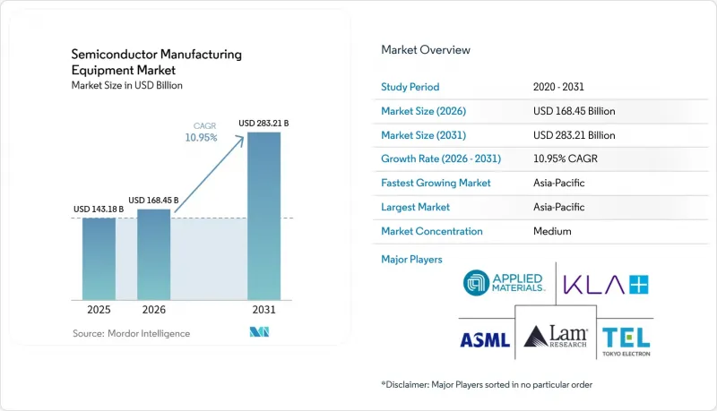
This report is Segmented by Equipment Type (Wafer Fab Equipment / Front-End Equipment, and More), by Device Type (Logic and Micro-Components, Memory, Analog, and More), by End-User (Integrated Device Manufacturers (IDMs), Foundries, and More), and by Geography (Asia-Pacific, Europe, and More). The Report Offers Market Size and Forecasts in Value (USD) for all the Above Segments.
Global Semiconductor Manufacturing Equipment Market Trends and Insights
AI, HBM, Chiplets, and Advanced Packaging Demand
AI accelerators, high-bandwidth memory, chiplets, and advanced packaging are changing the pattern of equipment investment. SEMI projected USD 52 billion in global 300 mm memory fab equipment spending for 2026, with DRAM equipment spending expected to reach USD 37 billion. The semiconductor manufacturing equipment market benefits from HBM production, which requires specialized processes for etch, deposition, fill, inspection, and packaging. These requirements add tool demand before considering any increase in memory output. Chiplet designs also increase the need for precise die placement, bonding, test, and inspection. This driver is strongest in Taiwan, South Korea, and North America, where leading logic and memory capacity is concentrated. It provides the semiconductor manufacturing equipment market with sustained exposure to high-value manufacturing and packaging investments.
Advanced Node Migration and Rising Process Complexity
The move toward 2 nm gate-all-around designs increases the number and precision of fabrication steps. SEMI expects foundry and logic wafer fab equipment spending to reach USD 78 billion in 2026, up 18.9% from 2025. Gate-all-around structures require more selective etch and deposition work than earlier FinFET designs. Each additional step can also increase the need for metrology and process-control equipment. Intel Foundry used ASML's High NA EUV system for a high-volume logic product in July 2026, demonstrating that new lithography platforms are entering production. The semiconductor manufacturing equipment market, therefore, benefits from higher equipment intensity as manufacturers move to more complex process nodes. This leaves the semiconductor manufacturing equipment market less dependent on new fab buildings alone.
Export Controls, Tariffs, and Trade Fragmentation
Export controls have narrowed the range of equipment and related technologies that can be supplied to certain destinations. In December 2024, the United States Bureau of Industry and Security added controls covering 24 types of semiconductor manufacturing equipment, 3 types of semiconductor development software, HBM-related rules, and 140 additions to the Entity List. A January 2025 interim final rule extended licensing requirements for certain advanced computing integrated circuits and covered manufacturing routes. These rules create compliance requirements for suppliers and customers across several countries. They can affect product configuration, customer qualification, shipment timing, and service arrangements. The semiconductor manufacturing equipment market also faces the risk that restrictions support the development of alternative domestic supply chains.
Other drivers and restraints analyzed in the detailed report include:
- Memory Technology Upgrades and HBM Capacity Expansion
- Government Fab Localization and Subsidy Programs
- Semiconductor Capex Cyclicality and Fab Investment Delays
For complete list of drivers and restraints, kindly check the Table Of Contents.
Segment Analysis
Front-end equipment accounted for 65.45% of the market share in 2025. It remained the main driver of spending because advanced logic and memory fabs require lithography, deposition, etch, cleaning, planarization, thermal processing, metrology, and inspection. SEMI forecasts wafer fab equipment spending of USD 143.9 billion in 2026, a 23.1% rise from 2025. The semiconductor manufacturing equipment market size is supported by leading-edge logic and memory capacity, as well as by more demanding process flows. Applied Materials introduced deposition and selective-etch systems in June 2026 for deep, narrow 3D structures used in advanced logic and memory. ASML also plans to continue expanding EUV and DUV capacity to serve customer demand. These actions show that front-end demand includes both new capacity and tool replacement at more advanced nodes.
Assembly, packaging, and test equipment registered the fastest 13.50% CAGR through 2031 and have become increasingly important as AI devices and HBM stacks require more complex back-end operations. SEMI reported that test equipment increased 55% in 2025 and projected USD 15.3 billion in test equipment sales for 2026. Packaging equipment also supports hybrid bonding, die attach, substrate inspection, and other specialized work. Applied Materials introduced systems for through-silicon via fill, microbump formation, and defect analysis in June 2026. Fab facility, automation, and support equipment remain necessary for greenfield sites that require chemical delivery, gas systems, material handling, and cleanroom infrastructure. Together, these activities broaden demand for equipment beyond the primary wafer-processing stage.
Complete Report Scope:
- By Equipment Type
- Wafer Fab Equipment / Front-End Equipment (lithography, deposition, etching, cleaning, CMP, thermal processing, front-end metrology & inspection equipment, etc.)
- Assembly and Packaging Equipment (die attach, wire bonding, flip-chip bonding, wafer bumping, thinning, dicing, molding, etc.)
- Semiconductor Test Equipment (automated test equipment, wafer probers, test handlers, burn-in equipment, and final test equipment)
- Fab Facility, Automation and Support Equipment (automation systems, wafer handling systems, AMHS, chemical & gas delivery systems, chillers, cleanroom support equipment, etc.)
- By Device Type
- Logic and Microcomponents (logic ICs, microprocessors, etc.)
- Memory (DRAM, NAND, HBM, NOR, etc.)
- Microprocessors (MPUs)
- Analog (Power management ICs, signal chain, interface Ics, etc.)
- Discrete and Power Devices (Diodes, transistors, MOSFETs, etc.)
- Sensors, MEMS and Optoelectronic Devices (Image sensors, MEMS sensors, etc.)
- By End User
- Integrated Device Manufacturers (IDMs)
- Foundries
- Outsourced Semiconductor Assembly and Test (OSAT) Companies
- Others (Research & Development (R&D) and Pilot Lines)
- By Geography
- North America
- United States
- Canada
- Mexico
- South America
- Brazil
- Rest of South America
- Europe
- Germany
- France
- Ireland
- Italy
- Netherlands
- Rest of Europe
- Asia-Pacific
- China
- Taiwan
- South Korea
- Japan
- Singapore
- India
- Rest of Asia-Pacific
- Middle East and Africa
- North America
Geography Analysis
Asia-Pacific accounted for 64.35% of the market share in 2025 and is expected to remain the largest regional market for semiconductor manufacturing equipment, registering a 12.30% CAGR, led by China, Taiwan, South Korea, and Japan, which together account for the majority of global equipment billings. Taiwan is projected to record USD 31.5 billion in semiconductor equipment billings, a 90% increase from 2024, driven by continued investments in advanced logic and advanced packaging capacity. South Korea is expected to reach USD 25.8 billion, up 26%, supported by expansions in HBM and DRAM capacity. Japan's billings are projected to increase by 22% to USD 9.5 billion, as domestic fabrication projects and its established semiconductor materials and equipment ecosystem sustain capital investment. China is expected to remain the world's largest equipment market, with USD 49.3 billion in billings, despite a marginal 0.5% decline, reflecting continued investment in mature-node manufacturing, specialty semiconductors, and domestic supply chain development.
North America is projected to record USD 10.9 billion in equipment billings, down 20% year over year. However, the construction and commissioning of new fabs supported by the CHIPS and Science Act are expected to drive higher equipment installations as projects advance from site development to production. Europe is expected to generate USD 2.9 billion in billings in 2025, a 41% decline from 2024. However, the European Chips Act continues to support strategic investments in semiconductor manufacturing and technology expansion across the region. Emerging manufacturing hubs, including India through the Semicon India Programme and Singapore through investments in advanced packaging and specialty semiconductors, are strengthening their positions within the global semiconductor manufacturing ecosystem. Looking ahead, SEMI projects China, Taiwan, and South Korea to remain the three largest semiconductor equipment markets through 2031, reflecting the continued concentration of global wafer fabrication capacity and advanced-node investments.
- Applied Materials, Inc.
- ASML Holding N.V.
- Lam Research Corporation
- Tokyo Electron Limited
- KLA Corporation
- SCREEN Holdings Co., Ltd.
- Advantest Corporation
- ASM International N.V.
- Teradyne, Inc.
- Hitachi High-Tech Corporation
- Onto Innovation Inc.
- Cohu, Inc.
- BE Semiconductor Industries N.V.
- EV Group
- Kokusai Electric Corporation
- ASMPT Limited
- ACM Research, Inc.
- Disco Corporation
- Canon Inc.
- Nikon Corporation
- Axcelis Technologies, Inc.
- Nova Ltd.
- Lasertec Corporation
- SUSS MicroTec SE
- Tokyo Seimitsu Co., Ltd. / ACCRETECH
Additional Benefits:
- The market estimate (ME) sheet in Excel format
- 3 months of analyst support
TABLE OF CONTENTS
1 INTRODUCTION
- 1.1 Study Assumptions and Market Definition
- 1.2 Scope of the Study
2 RESEARCH METHODOLOGY
3 EXECUTIVE SUMMARY
4 MARKET LANDSCAPE
- 4.1 Market Overview
- 4.2 Market Drivers
- 4.2.1 AI, HBM, Chiplets, and Advanced Packaging Demand
- 4.2.2 Advanced Node Migration and Rising Process Complexity
- 4.2.3 Memory Technology Upgrades and HBM Capacity Expansion
- 4.2.4 Government Fab Localization and Subsidy Programs
- 4.2.5 Multi-Region Fab Capacity Expansion
- 4.2.6 Mature-Node, Power Semiconductor, and Specialty Fab Investments
- 4.3 Market Restraints
- 4.3.1 Export Controls, Tariffs, and Trade Fragmentation
- 4.3.2 Semiconductor Capex Cyclicality and Fab Investment Delays
- 4.3.3 Supplier Bottlenecks in Optics, Vacuum, Precision Components, and Specialty Inputs
- 4.3.4 Extreme Tool Cost, Long Lead Times, and Long Payback Cycles
- 4.4 Value and Supply-Chain Analysis
- 4.5 Regulatory and Policy Landscape
- 4.6 Technology and Innovation Trends
- 4.7 Insights on Global Semiconductor Fab Expansion and Capacity Additions
- 4.8 Insights on AI and Automation in Semiconductor Manufacturing
- 4.9 Equipment Demand Outlook by Manufacturing Stage (Wafer fabrication, Assembly and packaging, Testing, Fab facility and automation)
- 4.10 Impact Assessment of Geopolitical Events on the Market
5 MARKET SIZE AND GROWTH FORECASTS (Value, In USD Billion)
- 5.1 By Equipment Type
- 5.1.1 Wafer Fab Equipment / Front-End Equipment (lithography, deposition, etching, cleaning, CMP, thermal processing, front-end metrology & inspection equipment, etc.)
- 5.1.2 Assembly and Packaging Equipment (die attach, wire bonding, flip-chip bonding, wafer bumping, thinning, dicing, molding, etc.)
- 5.1.3 Semiconductor Test Equipment (automated test equipment, wafer probers, test handlers, burn-in equipment, and final test equipment)
- 5.1.4 Fab Facility, Automation and Support Equipment (automation systems, wafer handling systems, AMHS, chemical & gas delivery systems, chillers, cleanroom support equipment, etc.)
- 5.2 By Device Type
- 5.2.1 Logic and Microcomponents (logic ICs, microprocessors, etc.)
- 5.2.2 Memory (DRAM, NAND, HBM, NOR, etc.)
- 5.2.3 Microprocessors (MPUs)
- 5.2.4 Analog (Power management ICs, signal chain, interface Ics, etc.)
- 5.2.5 Discrete and Power Devices (Diodes, transistors, MOSFETs, etc.)
- 5.2.6 Sensors, MEMS and Optoelectronic Devices (Image sensors, MEMS sensors, etc.)
- 5.3 By End User
- 5.3.1 Integrated Device Manufacturers (IDMs)
- 5.3.2 Foundries
- 5.3.3 Outsourced Semiconductor Assembly and Test (OSAT) Companies
- 5.3.4 Others (Research & Development (R&D) and Pilot Lines)
- 5.4 By Geography
- 5.4.1 North America
- 5.4.1.1 United States
- 5.4.1.2 Canada
- 5.4.1.3 Mexico
- 5.4.2 South America
- 5.4.2.1 Brazil
- 5.4.2.2 Rest of South America
- 5.4.3 Europe
- 5.4.3.1 Germany
- 5.4.3.2 France
- 5.4.3.3 Ireland
- 5.4.3.4 Italy
- 5.4.3.5 Netherlands
- 5.4.3.6 Rest of Europe
- 5.4.4 Asia-Pacific
- 5.4.4.1 China
- 5.4.4.2 Taiwan
- 5.4.4.3 South Korea
- 5.4.4.4 Japan
- 5.4.4.5 Singapore
- 5.4.4.6 India
- 5.4.4.7 Rest of Asia-Pacific
- 5.4.5 Middle East and Africa
- 5.4.1 North America
6 COMPETITIVE LANDSCAPE
- 6.1 Market Concentration
- 6.2 Strategic Moves
- 6.3 Market Share Analysis
- 6.4 Company Profiles (includes Global Level Overview, Market Level Overview, Core Segments, Financials as available, Strategic Information, Products and Services, Recent Developments)
- 6.4.1 Applied Materials, Inc.
- 6.4.2 ASML Holding N.V.
- 6.4.3 Lam Research Corporation
- 6.4.4 Tokyo Electron Limited
- 6.4.5 KLA Corporation
- 6.4.6 SCREEN Holdings Co., Ltd.
- 6.4.7 Advantest Corporation
- 6.4.8 ASM International N.V.
- 6.4.9 Teradyne, Inc.
- 6.4.10 Hitachi High-Tech Corporation
- 6.4.11 Onto Innovation Inc.
- 6.4.12 Cohu, Inc.
- 6.4.13 BE Semiconductor Industries N.V.
- 6.4.14 EV Group
- 6.4.15 Kokusai Electric Corporation
- 6.4.16 ASMPT Limited
- 6.4.17 ACM Research, Inc.
- 6.4.18 Disco Corporation
- 6.4.19 Canon Inc.
- 6.4.20 Nikon Corporation
- 6.4.21 Axcelis Technologies, Inc.
- 6.4.22 Nova Ltd.
- 6.4.23 Lasertec Corporation
- 6.4.24 SUSS MicroTec SE
- 6.4.25 Tokyo Seimitsu Co., Ltd. / ACCRETECH
7 MARKET OPPORTUNITIES AND FUTURE OUTLOOK
- 7.1 White-Space and Unmet-Need Assessment

