PUBLISHER: Mordor Intelligence | PRODUCT CODE: 2122910

PUBLISHER: Mordor Intelligence | PRODUCT CODE: 2122910
Semiconductor Laser - Market Share Analysis, Industry Trends & Statistics, Growth Forecasts (2026 - 2031)
According to Mordor Intelligence, the semiconductor laser market size is expected to increase from USD 9.17 billion in 2025 to USD 10.40 billion in 2026 and reach USD 17.64 billion by 2031, growing at a CAGR of 11.15% over 2026-2031.
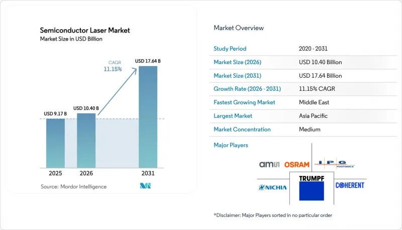
This report is Segmented by Wavelength (Infrared, Red, Green, Blue, and Ultraviolet), Laser Type (Edge-Emitting, VCSEL, Quantum Cascade, and Fiber), Application (Communication, Medical, Military and Defense, Industrial, Instrumentation and Sensor, and Automotive), Power Output (Below 100 MW, 100 MW To 1 W, 1 W To 5 W, and Above 5 W), and Geography. Market Forecasts are in Value (USD).
Global Semiconductor Laser Market Trends and Insights
Rapid Expansion of 3D Sensing in Consumer Electronics
VCSEL array shipments for time-of-flight and structured-light modules surged as smartphone vendors broadened facial authentication and augmented-reality features, with wall-plug efficiencies topping 45% and reliable operation up to 150 °C without active cooling . Sony leveraged its back-illuminated sensor expertise to co-package VCSEL dies and CMOS detectors, reducing module footprints by 30% and lowering unit costs to below USD 2 in high-volume orders. Android flagship adoption increased from 18% in 2023 to an estimated 42% in 2025, as manufacturers sought to secure payments and differentiate their products. Euro NCAP cabin-monitoring rules triggered dual-zone VCSEL illuminators that withstand temperatures ranging from -40 °C to +85 °C, thereby tightening epitaxial uniformity requirements. Wearables add another growth vector, with smart glasses and health monitors forecast to exceed 50 million units annually by 2028 as sub-5 mm VCSEL modules enable gesture recognition and non-contact heart-rate sensing.
Emerging Demand from Silicon Photonics Interconnects
Hyperscale operators transitioned from 400G to 800G Ethernet between 2024 and 2025, integrating heterogeneously bonded III-V lasers on silicon to achieve sub-3W lane power and coupling losses of below 0.5 dB. Co-packaged optics place laser arrays directly on switch ASICs, eliminating SerDes bottlenecks and cutting latency by 40 ns, an edge prized for AI training clusters. DARPA committed USD 203 million in 2025 to lift heterogeneous integration yields toward 95%. The current wall-plug efficiency hovers near 10%, falling short of the 20% thermal envelope for air-cooled racks, which has spurred research on quantum-dot gain media and photonic-crystal cavities aimed at achieving 15% by 2027. Kerr frequency combs are displacing discrete arrays, providing 80 channels from one micro-resonator and reducing transceiver bills of materials by 35% in metro networks.
Supply Chain Volatility of Compound Semiconductor Wafers
Four suppliers control 78% of global gallium-arsenide wafer capacity, leaving the semiconductor laser market exposed to sudden demand swings. China's August 2023 curbs on gallium and germanium stretched 6-inch substrate lead times from 12 to 26 weeks and pushed spot prices 40% higher by early 2024. Hyperscale buyers locked long-term indium-phosphide contracts, crowding smaller diode makers toward less flexible gallium-arsenide alternatives. Dual-sourcing requires 18-24 months of AEC-Q100 and Telcordia GR-468-CORE testing, which delays diversification. Scaling from 4- to 6-inch wafers remains capital-intensive; a single MOCVD reactor costs USD 4 million and needs 95% utilization for a 5-year payback.
Other drivers and restraints analyzed in the detailed report include:
- Proliferation of Semiconductor Laser Applications
- Government-Backed Photonics Manufacturing Initiatives
- Thermal Management Challenges at High Power Outputs
For complete list of drivers and restraints, kindly check the Table Of Contents.
Segment Analysis
Infrared lasers accounted for 42.5% of 2025 revenue, underpinning the semiconductor laser market through 850 nm and 1,550 nm devices that dominate consumer 3D sensing and long-haul fiber links . Ultraviolet variants, although smaller in absolute dollars, will climb at a 14.8% CAGR to 2031 on EUV lithography shipments and medical UV-curable prototyping, pointing to a rising semiconductor laser market size contribution from advanced manufacturing tools.
VCSEL-based infrared modules deliver circular beams that simplify coupling, while QCL-based mid-infrared sources provide tunability for gas sensing. Ultraviolet penetration remains cost-sensitive but emerging 266 nm diodes promise higher yields and longer lifetimes. Regulatory IEC 60825 Class 3B and Class 4 limits demand sophisticated interlocks above 5 mW, influencing design budgets and time to market. As advanced logic nodes migrate below 3 nm, lithography tool vendors will propel ultraviolet demand, reinforcing its double-digit climb within the semiconductor laser market.
VCSELs captured a 37.8% share, thanks to wafer-scale testing that reduces die cost below USD 0.50, thereby safeguarding their leadership in the semiconductor laser market. QCLs, however, are racing ahead at a 16.3% CAGR through 2031, as mid-infrared spectroscopy gains regulatory tailwinds, suggesting a growing impact on the semiconductor laser market size from environmental and defense programs.
Edge-emitting bars retain relevance for multi-kilowatt industrial cutting, yet their 6% CAGR lags. Fiber lasers, although technically outside the pure semiconductor classification, depend on diode pumping and maintain a 9% trajectory. Narrow-linewidth external-cavity diodes fill metrology niches requiring <1 MHz linewidth. Over the forecast period, design wins in automotive LiDAR and gas monitoring will help QCLs erode VCSEL dominance, diversifying revenue streams within the semiconductor laser market.
Complete Report Scope:
- By Wavelength
- Infrared Lasers
- Red Lasers
- Green Lasers
- Blue Lasers
- Ultraviolet Lasers
- By Laser Type
- Edge-Emitting Lasers (EEL)
- Vertical-Cavity Surface-Emitting Lasers (VCSEL)
- Quantum Cascade Lasers
- Fiber Lasers
- Other Types
- By Application
- Communication
- Medical
- Military and Defense
- Industrial
- Instrumentation and Sensor
- Automotive
- Other Applications
- By Power Output
- Below 100 mW
- 100 mW - 1 W
- 1 W - 5 W
- Above 5 W
- By Geography
- North America
- United States
- Canada
- Mexico
- Europe
- Germany
- United Kingdom
- France
- Italy
- Spain
- Russia
- Rest of Europe
- Asia-Pacific
- China
- Japan
- India
- South Korea
- Australia
- Rest of Asia-Pacific
- Middle East
- Saudi Arabia
- United Arab Emirates
- Turkey
- Rest of Middle East
- Africa
- South Africa
- Nigeria
- Rest of Africa
- South America
- Brazil
- Argentina
- Rest of South America
- North America
Geography Analysis
The Asia-Pacific region generated 48.2% of 2025 revenue, reflecting China's 60% share of global VCSEL epitaxial wafers and Japan's 200 million-unit annual diode output. Samsung's foundry-scale gallium-arsenide services trim wafer costs by 20%, while India's 25% subsidy attracts new assembly lines. Singapore, Hong Kong, and Tokyo data center expansions, which require 800 Gbit transceivers, are expected to support a 10.8% regional CAGR, keeping the Asia-Pacific region central to the semiconductor laser market.
North America remained a significant contributor to 2025 sales, driven by hyperscale cloud consumption, which comprises 40% of global silicon photonics shipments. The CHIPS Act will fund domestic epitaxial wafers; however, new fabs typically require 36 to 48 months to reach volume production. Canada's CAD 100 million photonics cluster and Mexico's duty-free equipment imports under USMCA strengthen continental resilience.
Europe remained a significant revenue contributor, anchored by Germany's TRUMPF and ams-OSRAM plus Fraunhofer R&D. Horizon funds and UK pilot lines enhance heterogeneous integration, while RoHS and REACH compliance add six-to-twelve-month qualification overhead. The Middle East's 12.9% CAGR is driven by NEOM's USD 500 billion investment, which incorporates LiDAR into mobility infrastructure. South America and Africa together supply 6% of the revenue, with Brazil's.
- Coherent Corp.
- Sharp Corporation
- Nichia Corporation
- IPG Photonics Corporation
- TT Electronics plc
- Sumitomo Electric Industries Ltd.
- Sheaumann Laser Inc.
- Newport Corporation (MKS Instruments Inc.)
- Panasonic Industry Co. Ltd.
- Rohm Co. Ltd.
- Hamamatsu Photonics K.K.
- Jenoptik AG
- TRUMPF Group
- ams-OSRAM AG
- Lumentum Holdings Inc.
- Broadcom Inc.
- Furukawa Electric Co. Ltd.
- Innolume GmbH
- MACOM Technology Solutions Holdings Inc.
- II-VI Incorporated (now part of Coherent)
Additional Benefits:
- The market estimate (ME) sheet in Excel format
- 3 months of analyst support
TABLE OF CONTENTS
1 INTRODUCTION
- 1.1 Study Assumptions and Market Definition
- 1.2 Scope of the Study
2 RESEARCH METHODOLOGY
3 EXECUTIVE SUMMARY
4 MARKET LANDSCAPE
- 4.1 Market Overview
- 4.2 Market Drivers
- 4.2.1 Proliferation of Semiconductor Laser Applications
- 4.2.2 Growth in Fiber Laser Adoption
- 4.2.3 Preference for Semiconductor Lasers over Other Light Sources
- 4.2.4 Rapid Expansion of 3D Sensing in Consumer Electronics
- 4.2.5 Emerging Demand from Silicon Photonics Interconnects
- 4.2.6 Government-Backed Photonics Manufacturing Initiatives
- 4.3 Market Restraints
- 4.3.1 Difficulties Regarding Reliability and Testing
- 4.3.2 Supply Chain Volatility of Compound Semiconductor Wafers
- 4.3.3 Thermal Management Challenges at High Power Outputs
- 4.3.4 Stringent Export Controls on Advanced Photonics
- 4.4 Industry Value Chain Analysis
- 4.5 Regulatory Landscape
- 4.6 Technological Outlook
- 4.7 Impact of Macroeconomic Factors
- 4.8 Porter's Five Forces Analysis
- 4.8.1 Threat of New Entrants
- 4.8.2 Bargaining Power of Suppliers
- 4.8.3 Bargaining Power of Buyers
- 4.8.4 Threat of Substitutes
- 4.8.5 Competitive Rivalry
5 MARKET SIZE AND GROWTH FORECASTS (VALUE)
- 5.1 By Wavelength
- 5.1.1 Infrared Lasers
- 5.1.2 Red Lasers
- 5.1.3 Green Lasers
- 5.1.4 Blue Lasers
- 5.1.5 Ultraviolet Lasers
- 5.2 By Laser Type
- 5.2.1 Edge-Emitting Lasers (EEL)
- 5.2.2 Vertical-Cavity Surface-Emitting Lasers (VCSEL)
- 5.2.3 Quantum Cascade Lasers
- 5.2.4 Fiber Lasers
- 5.2.5 Other Types
- 5.3 By Application
- 5.3.1 Communication
- 5.3.2 Medical
- 5.3.3 Military and Defense
- 5.3.4 Industrial
- 5.3.5 Instrumentation and Sensor
- 5.3.6 Automotive
- 5.3.7 Other Applications
- 5.4 By Power Output
- 5.4.1 Below 100 mW
- 5.4.2 100 mW - 1 W
- 5.4.3 1 W - 5 W
- 5.4.4 Above 5 W
- 5.5 By Geography
- 5.5.1 North America
- 5.5.1.1 United States
- 5.5.1.2 Canada
- 5.5.1.3 Mexico
- 5.5.2 Europe
- 5.5.2.1 Germany
- 5.5.2.2 United Kingdom
- 5.5.2.3 France
- 5.5.2.4 Italy
- 5.5.2.5 Spain
- 5.5.2.6 Russia
- 5.5.2.7 Rest of Europe
- 5.5.3 Asia-Pacific
- 5.5.3.1 China
- 5.5.3.2 Japan
- 5.5.3.3 India
- 5.5.3.4 South Korea
- 5.5.3.5 Australia
- 5.5.3.6 Rest of Asia-Pacific
- 5.5.4 Middle East
- 5.5.4.1 Saudi Arabia
- 5.5.4.2 United Arab Emirates
- 5.5.4.3 Turkey
- 5.5.4.4 Rest of Middle East
- 5.5.5 Africa
- 5.5.5.1 South Africa
- 5.5.5.2 Nigeria
- 5.5.5.3 Rest of Africa
- 5.5.6 South America
- 5.5.6.1 Brazil
- 5.5.6.2 Argentina
- 5.5.6.3 Rest of South America
- 5.5.1 North America
6 COMPETITIVE LANDSCAPE
- 6.1 Market Concentration
- 6.2 Strategic Moves
- 6.3 Market Share Analysis
- 6.4 Company Profiles (includes Global level Overview, Market level overview, Core Segments, Financials as available, Strategic Information, Market Rank/Share for key companies, Products and Services, and Recent Developments)
- 6.4.1 Coherent Corp.
- 6.4.2 Sharp Corporation
- 6.4.3 Nichia Corporation
- 6.4.4 IPG Photonics Corporation
- 6.4.5 TT Electronics plc
- 6.4.6 Sumitomo Electric Industries Ltd.
- 6.4.7 Sheaumann Laser Inc.
- 6.4.8 Newport Corporation (MKS Instruments Inc.)
- 6.4.9 Panasonic Industry Co. Ltd.
- 6.4.10 Rohm Co. Ltd.
- 6.4.11 Hamamatsu Photonics K.K.
- 6.4.12 Jenoptik AG
- 6.4.13 TRUMPF Group
- 6.4.14 ams-OSRAM AG
- 6.4.15 Lumentum Holdings Inc.
- 6.4.16 Broadcom Inc.
- 6.4.17 Furukawa Electric Co. Ltd.
- 6.4.18 Innolume GmbH
- 6.4.19 MACOM Technology Solutions Holdings Inc.
- 6.4.20 II-VI Incorporated (now part of Coherent)
7 MARKET OPPORTUNITIES AND FUTURE OUTLOOK
- 7.1 White-Space and Unmet-Need Assessment

