PUBLISHER: Mordor Intelligence | PRODUCT CODE: 2124127

PUBLISHER: Mordor Intelligence | PRODUCT CODE: 2124127
Photoresist - Market Share Analysis, Industry Trends & Statistics, Growth Forecasts (2026 - 2031)
According to Mordor Intelligence, the photoresist market size is projected to be USD 2.91 billion in 2025, USD 3.24 billion in 2026, and reach USD 5.53 billion by 2031, growing at a CAGR of 11.31% from 2026 to 2031.
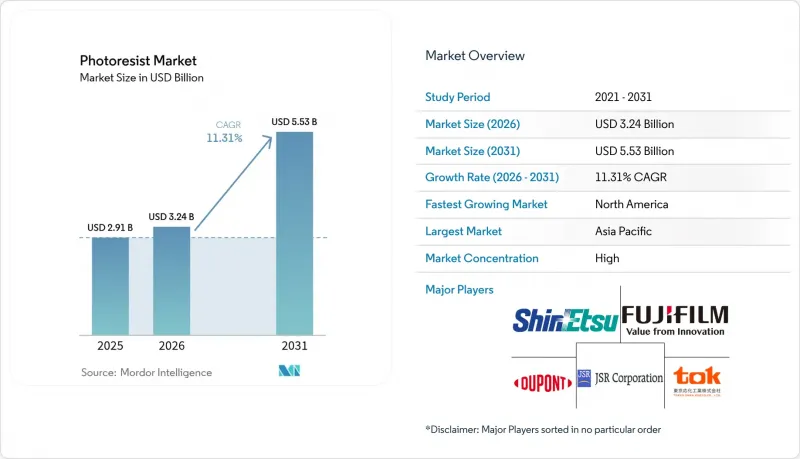
This report is Segmented by Resist Type (ArF Immersion, Arf Dry, Krf, G-Line, I-Line, EUV Metal-Oxide, and Other Types), Tone (Positive and Negative), Application (Semiconductors, Advanced Packaging, Displays, Pcbs, MEMS, and Other), End-User (Electronics, Automotive, Aerospace, CPG, and Other), and Geography (Asia-Pacific, North America, Europe, and More). Market Forecasts are in Value (USD).
Global Photoresist Market Trends and Insights
Growing Demand from Semiconductor and AI Accelerators
Worldwide capital expenditure on wafer-fabrication equipment is slated to rise between 2026 and 2028, reflecting heavier AI-accelerator requirements in hyperscale data centers. Alphabet doubled its outlays for tensor-processing units in 2025, raising overlay-tolerance specifications that directly increase photoresist consumption per wafer. Intel's Lunar Lake processors integrate on-package memory using through-silicon vias, adding specialized redistribution-layer lithography steps that further drive resist intensity. Because advanced chiplet architectures raise the number of masking passes, resist demand is decoupling from smartphone unit cycles, sustaining growth even as handset shipments level off. TSMC locked in multiyear EUV-resist supply agreements for its Arizona fab two years before ramp to guarantee chemistry availability, underscoring the material's strategic role.
Accelerated EUV Lithography Adoption and High-NA Roadmap
In 2024, ASML rolled out its inaugural 0.55 numerical-aperture High-NA EUV scanner, an innovation that facilitates 8-nanometer half-pitch patterning, sidestepping the expenses of multi-patterning. Intel has pledged allegiance to High-NA for its 18-angstrom node, while Samsung and TSMC eye sub-3-nanometer integration post-2027. High-NA optics grapple with absorption coefficients exceeding 10 µm-1 at 13.5 nm. This is a challenge zone, as traditional chemically-amplified compositions falter with line-edge roughness. While metal-oxide alternatives, derived from tin-oxo clusters, satisfy absorption criteria, they bring forth stochastic defects. This challenge has spurred a collaborative effort between JSR and Lam Research, aiming to reduce defect density. Their co-optimization strategy forges a closer bond between resist suppliers and tool manufacturers, setting a higher barrier for industry newcomers.
Stringent HSE Rules on Solvents and Photo-Acid Generators
The U.S. EPA classified several PFAS solvent families as hazardous in 2024, mandating costly abatement or substitution at resist-blending plants within two years. The EU added triphenylsulfonium salts to its REACH authorization list in 2025, imposing sunset dates that accelerate reformulation campaigns and tilt research and development budgets away from high-performance chemistry toward compliance work. Tokyo Ohka Kogyo disclosed that a significant amount of its 2025 research and development spend was consumed by solvent reformulations, reinforcing a trend where only the largest suppliers can carry simultaneous compliance and node-transition programs. Industry lobbying secured a five-year carve-out for EUV resists, yet environmental-advocacy lawsuits threaten to shorten the grace period, injecting regulatory uncertainty into capacity-planning models.
Other drivers and restraints analyzed in the detailed report include:
- 5G/IoT Proliferation Expanding Wafer Starts
- Government Fab-Incentive Programs (US/EU CHIPS Acts)
- Supply-Chain Concentration and Export-Control Exposure
For complete list of drivers and restraints, kindly check the Table Of Contents.
Segment Analysis
ArF immersion held 31.92% of the photoresist market share in 2025, while EUV metal-oxide and dry resists are forecast to expand at a 12.94% CAGR, capturing incremental photoresist market size from sub-5-nanometer logic nodes.
Chemically amplified ArF immersion remains the price-performance leader for 28- to 7-nanometer automotive and connectivity chips, delivering solid yields on fully-depreciated scanners. KrF, g-line, and i-line formulations persist in analog and MEMS lines, buffering suppliers against EUV-cycle volatility. Conversely, tin- and hafnium-based metal-oxide systems enable the High-NA EUV roadmap with 2-nm line-edge roughness performance, albeit at higher exposure dose and cost. Toolmakers and chemistry suppliers are co-designing deposition-etch sequences that promise to cut cycle time, which, if realized at scale, could swing total cost of ownership toward metal-oxide in the outer years of the forecast.
Positive-tone chemistries commanded 71.51% share in 2025, yet negative-tone resists are climbing at an 11.38% CAGR, driven by their robustness in self-aligned double-patterning and EUV contact layers.
Advanced packaging flows favor the thicker films and aqueous developers of positive-tone materials, but sub-7-nanometer logic increasingly uses negative-tone for via layers that would otherwise collapse under rinse stress. Suppliers are releasing switchable-tone hybrids that toggle through bake-temperature adjustments, allowing fabs to maintain a single base chemistry across multiple layers and dilute qualification overhead, thereby augmenting photoresist market size gains from tone diversification.
Complete Report Scope:
- By Resist Type
- ArF Immersion
- ArF Dry
- KrF
- G-Line
- I-Line
- EUV Metal-Oxide and Dry Resists
- Other Types
- By Tone
- Positive
- Negative
- By Application
- Semiconductors and ICs
- Advanced Packaging (Fan-Out WLP, RDL)
- Flat-Panel Displays (LCD/OLED)
- Printed Circuit Boards
- MEMS and Sensors
- Other Applications
- By End-User Industry
- Electronics and Electricals
- Automotive and Mobility
- Aerospace and Defense
- Consumer Packaged Goods (Packaging)
- Other Industries
- By Geography
- Asia-Pacific
- China
- Japan
- South Korea
- Taiwan
- India
- Rest of Asia-Pacific
- North America
- United States
- Canada
- Mexico
- Europe
- Germany
- United Kingdom
- France
- Italy
- Russia
- Rest of Europe
- South America
- Brazil
- Argentina
- Rest of South America
- Middle-East and Africa
- Saudi Arabia
- United Arab Emirates
- South Africa
- Rest of Middle-East and Africa
- Asia-Pacific
Geography Analysis
Asia-Pacific captured 72.34% of the photoresist market in 2025. This dominance is largely attributed to Taiwanese and South Korean fabs, which handle the majority of the world's leading-edge wafers. Meanwhile, North America is set to increase its foothold, with an 11.49% CAGR. Thanks to the CHIPS Act, projects in Arizona, Ohio, and Texas are on track to contribute significantly to the global 2- to 5-nm capacity by 2028. This surge is prompting suppliers to establish blending lines closer to their customers.
Europe is experiencing moderate growth, driven by Intel's investment in Magdeburg and a joint venture between STMicroelectronics and GlobalFoundries in France. However, Europe still relies on imports for its EUV resists. China faces challenges due to export controls on advanced photoresists. As a countermeasure, it's aggressively expanding its 28-nm capacity and is heavily investing in ArF dry and KrF chemistries. Yet, the nation grapples with developing its domestic High-NA capability.
India and the Middle East are emerging as significant players in the photoresist landscape. Micron's assembly-test facility in Gujarat and Tata-Powerchip's fab agreement signify India's inaugural moves into wafer fabrication. Concurrently, Abu Dhabi's Mubadala is spearheading a packaging cluster, initially dependent on imported KrF resists. While these developments offer suppliers a chance to diversify away from the Asia-Pacific stronghold, the immediate volume impact is minimal.
- ALLRESIST GmbH
- Asahi Kasei Corporation
- Avantor, Inc.
- Brewer Science, Inc.
- DJ MicroLaminates
- DONGJIN SEMICHEM CO. LTD
- DuPont
- Eternal Materials Co., Ltd.
- FUJIFILM Corporation
- Inpria
- Jiangsu Nata Opto-electronic Material Co., Ltd.
- JSR Corporation
- Kolon Industries, Inc.
- LG Chem
- Merck KGaA
- micro resist technology GmbH
- Microchemicals GmbH
- SEMI
- Shin-Etsu Chemical Co., Ltd.
- Sumitomo Chemical Co., Ltd.
- TOKYO OHKA KOGYO CO., LTD.
Additional Benefits:
- The market estimate (ME) sheet in Excel format
- 3 months of analyst support
TABLE OF CONTENTS
1 Introduction
- 1.1 Study Assumptions and Market Definition
- 1.2 Scope of the Study
2 Research Methodology
3 Executive Summary
4 Market Landscape
- 4.1 Market Overview
- 4.2 Market Drivers
- 4.2.1 Growing demand from semiconductor and AI accelerators
- 4.2.2 Accelerated EUV lithography adoption and High-NA roadmap
- 4.2.3 5G/IoT proliferation expanding wafer starts
- 4.2.4 Government fab-incentive programs (US/EU Chips Acts)
- 4.2.5 Metal-oxide dry-deposited resists boosting EUV throughput
- 4.3 Market Restraints
- 4.3.1 Stringent HSE rules on solvents and photo-acid generators
- 4.3.2 Supply-chain concentration and export-control exposure
- 4.3.3 Yield risk from stochastic defects in sub-10 nm patterning
- 4.4 Value Chain Analysis
- 4.5 Regulatory Landscape
- 4.6 Porter's Five Forces
- 4.6.1 Bargaining Power of Suppliers
- 4.6.2 Bargaining Power of Buyers
- 4.6.3 Threat of New Entrants
- 4.6.4 Threat of Substitutes
- 4.6.5 Degree of Competition
5 Market Size and Growth Forecasts (Value)
- 5.1 By Resist Type
- 5.1.1 ArF Immersion
- 5.1.2 ArF Dry
- 5.1.3 KrF
- 5.1.4 G-Line
- 5.1.5 I-Line
- 5.1.6 EUV Metal-Oxide and Dry Resists
- 5.1.7 Other Types
- 5.2 By Tone
- 5.2.1 Positive
- 5.2.2 Negative
- 5.3 By Application
- 5.3.1 Semiconductors and ICs
- 5.3.2 Advanced Packaging (Fan-Out WLP, RDL)
- 5.3.3 Flat-Panel Displays (LCD/OLED)
- 5.3.4 Printed Circuit Boards
- 5.3.5 MEMS and Sensors
- 5.3.6 Other Applications
- 5.4 By End-User Industry
- 5.4.1 Electronics and Electricals
- 5.4.2 Automotive and Mobility
- 5.4.3 Aerospace and Defense
- 5.4.4 Consumer Packaged Goods (Packaging)
- 5.4.5 Other Industries
- 5.5 By Geography
- 5.5.1 Asia-Pacific
- 5.5.1.1 China
- 5.5.1.2 Japan
- 5.5.1.3 South Korea
- 5.5.1.4 Taiwan
- 5.5.1.5 India
- 5.5.1.6 Rest of Asia-Pacific
- 5.5.2 North America
- 5.5.2.1 United States
- 5.5.2.2 Canada
- 5.5.2.3 Mexico
- 5.5.3 Europe
- 5.5.3.1 Germany
- 5.5.3.2 United Kingdom
- 5.5.3.3 France
- 5.5.3.4 Italy
- 5.5.3.5 Russia
- 5.5.3.6 Rest of Europe
- 5.5.4 South America
- 5.5.4.1 Brazil
- 5.5.4.2 Argentina
- 5.5.4.3 Rest of South America
- 5.5.5 Middle-East and Africa
- 5.5.5.1 Saudi Arabia
- 5.5.5.2 United Arab Emirates
- 5.5.5.3 South Africa
- 5.5.5.4 Rest of Middle-East and Africa
- 5.5.1 Asia-Pacific
6 Competitive Landscape
- 6.1 Market Concentration
- 6.2 Strategic Moves
- 6.3 Market Share (%)/Ranking Analysis
- 6.4 Company Profiles (includes Global-level Overview, Market-level Overview, Core Segments, Financials, Strategic Information, Products and Services, Recent Developments)
- 6.4.1 ALLRESIST GmbH
- 6.4.2 Asahi Kasei Corporation
- 6.4.3 Avantor, Inc.
- 6.4.4 Brewer Science, Inc.
- 6.4.5 DJ MicroLaminates
- 6.4.6 DONGJIN SEMICHEM CO. LTD
- 6.4.7 DuPont
- 6.4.8 Eternal Materials Co., Ltd.
- 6.4.9 FUJIFILM Corporation
- 6.4.10 Inpria
- 6.4.11 Jiangsu Nata Opto-electronic Material Co., Ltd.
- 6.4.12 JSR Corporation
- 6.4.13 Kolon Industries, Inc.
- 6.4.14 LG Chem
- 6.4.15 Merck KGaA
- 6.4.16 micro resist technology GmbH
- 6.4.17 Microchemicals GmbH
- 6.4.18 SEMI
- 6.4.19 Shin-Etsu Chemical Co., Ltd.
- 6.4.20 Sumitomo Chemical Co., Ltd.
- 6.4.21 TOKYO OHKA KOGYO CO., LTD.
7 Market Opportunities and Future Outlook
- 7.1 White-space and Unmet-Need Assessment

