PUBLISHER: Mordor Intelligence | PRODUCT CODE: 2124831

PUBLISHER: Mordor Intelligence | PRODUCT CODE: 2124831
Transistor - Market Share Analysis, Industry Trends & Statistics, Growth Forecasts (2026 - 2031)
According to Mordor Intelligence, the transistor market size in 2026 is estimated at USD 20.02 billion, growing from 2025 value of USD 18.63 billion with 2031 projections showing USD 28.66 billion, growing at 7.46% CAGR over 2026-2031.
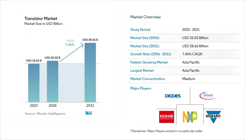
This report is Segmented by Transistor Type (Bipolar Junction Transistors (BJT), and More), Material (Silicon (Si), and More), Technology Node (Greater Than Equal To 65 Nm, and More), Packaging Type (Through-Hole, Surface-Mount, and More), End-User Industry (Consumer Electronics, Information and Communication Technology, and More), and Geography. The Market Forecasts are Provided in Terms of Value (USD).
Global Transistor Market Trends and Insights
Surging Demand for Power-Efficient Mobile SoCs
Mobile system-on-chip suppliers are lengthening transistor counts to integrate AI accelerators that execute on-device inference tasks without draining batteries. Chip architectures blend high-performance logic with analog blocks optimized for standby below 10 mW, shifting purchasing criteria from unit price to joules-per-operation. TSMC's 3 nm production lines entered mass production during 2025 mainly to serve smartphone SoCs, underscoring how node migration remains anchored in mobility workloads. Heterogeneous integration is reinforcing wafer-level packaging adoption as designers co-locate neural-processing cores and power-management circuitry on a single substrate. Although global smartphone shipments plateaued, rising silicon per handset is sustaining revenue growth across the transistor market.
Rapid Electrification of Transportation and Charging Infrastructure
Electric vehicles embed roughly 10 times more semiconductors than combustion models, most of which are high-current transistors handling traction inverters, on-board chargers, and DC-DC converters. The industry shift from 400 V to 800 V systems exceeds the safe-operating area of silicon devices, prompting automakers to specify SiC MOSFETs and IGBT modules rated at 1,200 V. Toshiba's new 300 mm facility aims to triple automotive-grade power semiconductor output, illustrating supplier responses to this long-cycle opportunity. Public fast-charger rollouts add further upside, as each station integrates multiple IGBT stacks and gate drivers. Qualification to AEC-Q100 extends design cycles by up to two years, creating a persistent gap between demand visibility and supply availability that underpins healthy pricing.
Quantum-Tunneling Limits Below 3 nm Nodes
Sub-3 nm geometries experience prohibitive leakage due to quantum tunneling, eroding the energy-delay benefit that historically justified node shrinks. Gate-all-around nanosheet transistors partially mitigate electrostatic loss yet demand intricate patterning sequences and expensive EUV multi-patterning steps. Foundries are therefore combining modest gate-length reductions with system-level innovations such as 3D stacking and chiplets to extend performance roadmaps rather than chasing pure lithographic scaling. The cost of a single sub-3 nm mask set now exceeds USD 10 million, meaning only the highest-volume consumer and cloud processors can amortize tooling expenses.
Other drivers and restraints analyzed in the detailed report include:
- AI/ML Inference at the Edge Driving Discrete Power Devices
- 5G-to-6G RF Front-End Upgrades
- Supply-Chain Concentration in Taiwan and South China
For complete list of drivers and restraints, kindly check the Table Of Contents.
Segment Analysis
Global IGBT revenue is projected to advance at 8.66% CAGR between 2026 and 2031, outpacing overall transistor market growth as e-mobility and renewable inverters demand high-efficiency switching components. The legacy BJT category retained 48.35% share of the transistor market size in 2025 by serving cost-sensitive consumer and industrial designs that do not need fast switching or extreme voltage tolerance. Suppliers are leveraging wafer-level packages to drive IGBT current ratings beyond 1,000 A while keeping switching loss at competitive levels.
Automotive safety standards, including ISO 26262, elevate barriers to entry by mandating extended mission-profile testing, a factor that supports premium pricing and reinforces moderate industry concentration. Nexperia's USD 200 million expansion into GaN and SiC processes aligns with customer roadmaps seeking alternative materials that can surpass the ruggedness limits of silicon IGBT structures. Field-effect transistors remain indispensable in logic applications, but their share gains are modest as node scaling slows and discrete counts plateau in smartphones and PCs.
Silicon kept 68.85% of the 2025 transistor market share, yet silicon-carbide devices are forecast to log the highest 8.86% CAGR to 2031 as traction inverters, solar inverters, and industrial drives transition to 1,200 V designs that reward lower switching loss. Gallium-nitride's niche in RF and fast-charger power stages is expanding, although substrate cost and wafer yield remain hurdles to mass penetration.
Government incentives, such as dedicated CHIPS Act grants for SiC pilot lines, ease upfront costs for domestic fabs and shorten the payback period on crystal-growth investments. Still, wide-bandgap wafer yields trail silicon by 20-30 percentage points, inflating die cost and confining adoption to applications where performance benefits justify premiums. Lab demonstrations of SiC JFET audio amplifiers highlight the broadening scope beyond power conversion, signaling future diversification paths for wide-bandgap suppliers.
Complete Report Scope:
- By Transistor Type
- Bipolar Junction Transistors (BJT)
- Field Effect Transistors (FET)
- Insulated Gate Bipolar Transistors (IGBT)
- Heterojunction Bipolar Transistors (HBT)
- By Material
- Silicon (Si)
- Silicon Carbide (SiC)
- Gallium Nitride (GaN)
- Germanium (Ge)
- By Technology Node
- Greater than Equal to 65 nm
- 45 - 28 nm
- 22 - 16 nm
- 14 - 10 nm
- Less than 10 nm
- By Packaging Type
- Through-Hole
- Surface-Mount
- Chip-Scale Package (CSP)
- Wafer-Level Package (WLP)
- By End-User Industry
- Consumer Electronics
- Information and Communication Technology
- Automotive and Transportation
- Industrial Manufacturing
- Energy and Power
- Aerospace and Defense
- Healthcare and Medical Devices
- By Geography
- North America
- United States
- Canada
- Mexico
- South America
- Brazil
- Argentina
- Colombia
- Rest of South America
- Europe
- United Kingdom
- Germany
- France
- Italy
- Spain
- Rest of Europe
- Asia-Pacific
- China
- Japan
- South Korea
- India
- Rest of Asia-Pacific
- Middle East and Africa
- Middle East
- Saudi Arabia
- United Arab Emirates
- Rest of Middle East
- Africa
- South Africa
- Egypt
- Rest of Africa
- Middle East
- North America
Geography Analysis
Asia-Pacific contributed 55.90% revenue in 2025 and is forecast to record a 10.62% CAGR to 2031. China's domestic foundries are scaling 28 nm and 14 nm lines under policy mandates, yet leading-edge constraints drive procurement from Taiwanese and South Korean fabs. India's production-linked incentive program has attracted multiple OSAT announcements, but logistics and skilled-labor gaps still temper near-term output. Japan maintains a critical role in photoresist, silicon-wafer, and deposition-tool supply, cushioning its transistor market relevance despite limited wafer-fab capacity. Emerging Southeast-Asian hubs such as Vietnam and Malaysia gain as second-source alternatives when multinationals diversify away from coastal China.
North America benefits from cloud-data-center expansion, electric-vehicle assembly growth, and defense-program mandates that prioritize domestic sourcing. The CHIPS Act's USD 52 billion allocation has unlocked multi-fab investments by TSMC, Samsung, and Intel, improving long-term supply security. Canada's focus on 5G infrastructure and battery-electric buses spurs specialized demand for RF and high-power devices, while Mexico's EMS clusters near the U.S. border attract transistor assembly lines that service automotive Tier-1 suppliers. Regional policy emphasis on supply-chain resilience supports a price premium that partially offsets elevated labor and construction costs.
Europe's transistor market gravitates around Germany's e-mobility shift, France's aerospace sector and the region-wide Green Deal that penalizes inefficient power conversion. Germany's OEMs are solo-sourcing SiC devices to stabilize inverter roadmaps, while French defense programs specify radiation-hardened transistors that endure harsh cosmic-ray environments. The European Chips Joint Undertaking funds advanced-node pilot lines with a dual objective: strategic autonomy and measurable carbon-footprint reduction. Brexit-related trade frictions prompt British OEMs to dual-source assemblies from continental OSATs, creating share opportunities for local suppliers in the Benelux corridor.
- onsemi Corporation
- Infineon Technologies AG
- STMicroelectronics N.V.
- Texas Instruments Incorporated
- Vishay Intertechnology, Inc.
- Diodes Incorporated
- NXP Semiconductors N.V.
- Renesas Electronics Corporation
- Linear Integrated Systems, Inc.
- ROHM Co., Ltd.
- Toshiba Electronic Devices and Storage Corporation
- Microchip Technology Inc.
- Broadcom Inc.
- Samsung Electronics Co., Ltd.
- Fuji Electric Co., Ltd.
- Mitsubishi Electric Corporation
- Alpha and Omega Semiconductor Limited
- Qorvo, Inc.
- Wolfspeed, Inc.
- Analog Devices, Inc.
Additional Benefits:
- The market estimate (ME) sheet in Excel format
- 3 months of analyst support
TABLE OF CONTENTS
1 INTRODUCTION
- 1.1 Study Assumptions and Market Definition
- 1.2 Scope of the Study
2 RESEARCH METHODOLOGY
3 EXECUTIVE SUMMARY
4 MARKET LANDSCAPE
- 4.1 Market Overview
- 4.2 Market Drivers
- 4.2.1 Surging demand for power-efficient mobile SoCs
- 4.2.2 Rapid electrification of transportation and charging infrastructure
- 4.2.3 AI/ML inference at the edge driving discrete power devices
- 4.2.4 5G?to-6G RF front-end upgrades
- 4.2.5 Government incentives for wide-band-gap fabs (SiC, GaN)
- 4.2.6 Adoption of advanced packaging (chip-let, 3D stacking)
- 4.3 Market Restraints
- 4.3.1 Quantum-tunnelling limits below 3 nm nodes
- 4.3.2 Supply-chain concentration in Taiwan and South-China
- 4.3.3 Rising fab construction CAPEX amid talent shortages
- 4.3.4 High qualification cost for automotive-grade devices
- 4.4 Industry Supply Chain Analysis
- 4.5 Regulatory Landscape
- 4.6 Technological Outlook
- 4.7 Porter's Five Forces Analysis
- 4.7.1 Threat of New Entrants
- 4.7.2 Bargaining Power of Buyers
- 4.7.3 Bargaining Power of Suppliers
- 4.7.4 Threat of Substitute Products
- 4.7.5 Intensity of Competitive Rivalry
5 MARKET SIZE AND GROWTH FORECASTS (VALUE)
- 5.1 By Transistor Type
- 5.1.1 Bipolar Junction Transistors (BJT)
- 5.1.2 Field Effect Transistors (FET)
- 5.1.3 Insulated Gate Bipolar Transistors (IGBT)
- 5.1.4 Heterojunction Bipolar Transistors (HBT)
- 5.2 By Material
- 5.2.1 Silicon (Si)
- 5.2.2 Silicon Carbide (SiC)
- 5.2.3 Gallium Nitride (GaN)
- 5.2.4 Germanium (Ge)
- 5.3 By Technology Node
- 5.3.1 Greater than Equal to 65 nm
- 5.3.2 45 - 28 nm
- 5.3.3 22 - 16 nm
- 5.3.4 14 - 10 nm
- 5.3.5 Less than 10 nm
- 5.4 By Packaging Type
- 5.4.1 Through-Hole
- 5.4.2 Surface-Mount
- 5.4.3 Chip-Scale Package (CSP)
- 5.4.4 Wafer-Level Package (WLP)
- 5.5 By End-User Industry
- 5.5.1 Consumer Electronics
- 5.5.2 Information and Communication Technology
- 5.5.3 Automotive and Transportation
- 5.5.4 Industrial Manufacturing
- 5.5.5 Energy and Power
- 5.5.6 Aerospace and Defense
- 5.5.7 Healthcare and Medical Devices
- 5.6 By Geography
- 5.6.1 North America
- 5.6.1.1 United States
- 5.6.1.2 Canada
- 5.6.1.3 Mexico
- 5.6.2 South America
- 5.6.2.1 Brazil
- 5.6.2.2 Argentina
- 5.6.2.3 Colombia
- 5.6.2.4 Rest of South America
- 5.6.3 Europe
- 5.6.3.1 United Kingdom
- 5.6.3.2 Germany
- 5.6.3.3 France
- 5.6.3.4 Italy
- 5.6.3.5 Spain
- 5.6.3.6 Rest of Europe
- 5.6.4 Asia-Pacific
- 5.6.4.1 China
- 5.6.4.2 Japan
- 5.6.4.3 South Korea
- 5.6.4.4 India
- 5.6.4.5 Rest of Asia-Pacific
- 5.6.5 Middle East and Africa
- 5.6.5.1 Middle East
- 5.6.5.1.1 Saudi Arabia
- 5.6.5.1.2 United Arab Emirates
- 5.6.5.1.3 Rest of Middle East
- 5.6.5.2 Africa
- 5.6.5.2.1 South Africa
- 5.6.5.2.2 Egypt
- 5.6.5.2.3 Rest of Africa
- 5.6.5.1 Middle East
- 5.6.1 North America
6 COMPETITIVE LANDSCAPE
- 6.1 Market Concentration
- 6.2 Strategic Moves
- 6.3 Market Share Analysis
- 6.4 Company Profiles (includes Global level Overview, Market level overview, Core Segments, Financials as available, Strategic Information, Market Rank/Share for key companies, Products and Services, and Recent Developments)
- 6.4.1 onsemi Corporation
- 6.4.2 Infineon Technologies AG
- 6.4.3 STMicroelectronics N.V.
- 6.4.4 Texas Instruments Incorporated
- 6.4.5 Vishay Intertechnology, Inc.
- 6.4.6 Diodes Incorporated
- 6.4.7 NXP Semiconductors N.V.
- 6.4.8 Renesas Electronics Corporation
- 6.4.9 Linear Integrated Systems, Inc.
- 6.4.10 ROHM Co., Ltd.
- 6.4.11 Toshiba Electronic Devices and Storage Corporation
- 6.4.12 Microchip Technology Inc.
- 6.4.13 Broadcom Inc.
- 6.4.14 Samsung Electronics Co., Ltd.
- 6.4.15 Fuji Electric Co., Ltd.
- 6.4.16 Mitsubishi Electric Corporation
- 6.4.17 Alpha and Omega Semiconductor Limited
- 6.4.18 Qorvo, Inc.
- 6.4.19 Wolfspeed, Inc.
- 6.4.20 Analog Devices, Inc.
7 MARKET OPPORTUNITIES AND FUTURE OUTLOOK
- 7.1 White-Space and Unmet-Need Assessment

