PUBLISHER: Mordor Intelligence | PRODUCT CODE: 2154206

PUBLISHER: Mordor Intelligence | PRODUCT CODE: 2154206
Wet Chemicals For Electronics and Semiconductor Applications - Market Share Analysis, Industry Trends & Statistics, Growth Forecasts (2026 - 2031)
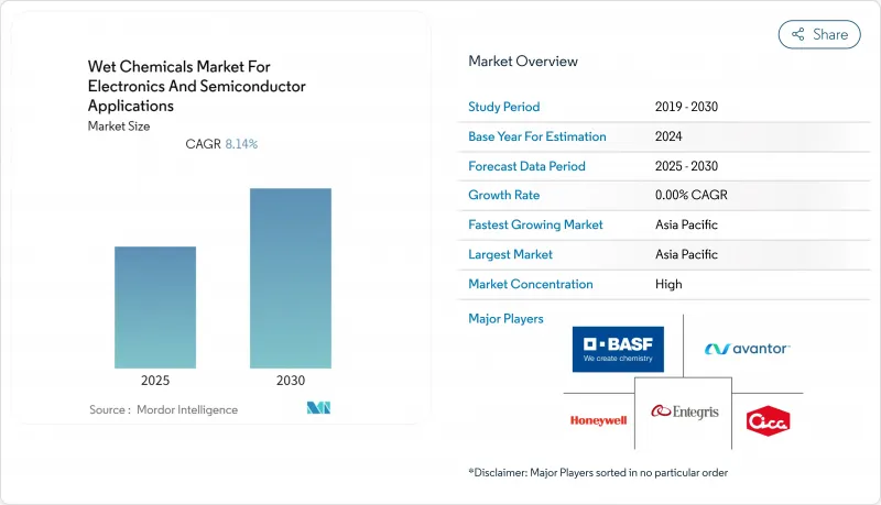
According to Mordor Intelligence, the wet chemicals for Electronics and Semiconductor Applications Market size was valued at USD 4.56 billion in 2025 and is estimated to grow from USD 4.89 billion in 2026 to reach USD 6.93 billion by 2031, at a CAGR of 7.23% during the forecast period (2026-2031).
Global Wet Chemicals For Electronics and Semiconductor Applications Market Trends and Insights
Expansion of Advanced-Node and 3D Semiconductor Fabrication
The wet chemicals for electronics and semiconductor applications market benefits from 3D NOT AND (NAND) and gate-all-around logic architectures, which add process steps to each wafer rather than merely reducing feature sizes. A 3 nm wafer moves through more than 600 process steps, with 15%-20% involving dedicated cleaning stages using dilute hydrofluoric acid, ammonium hydroxide-peroxide, and hydrochloric acid-peroxide formulations. Leading memory producers have moved beyond 200 stacked layers in 3D NAND, so each additional layer adds etching cycles and associated cleaning needs. Taiwan Semiconductor Manufacturing Company (TSMC) provided 2026 capital expenditure guidance of USD 52 billion-USD 56 billion for 2 nm capacity and advanced packaging facilities in Taiwan, Arizona, and Japan. Each new sub-7 nm fab can therefore become a larger recurring chemicals customer even when wafer output does not rise at the same rate as chemical use. Hybrid bonding adds surface preparation, post-bond cleaning, and through-silicon-via fill needs, broadening the role of wet chemistry beyond front-end wafer manufacturing.
AI, High-Performance Computing, 5G and Automotive Semiconductor Demand
The wet chemicals for electronics and semiconductor applications market gains support from artificial intelligence (AI) accelerators, high-performance computing processors, 5G equipment, and automotive chips. TSMC reported that AI accelerators and high-performance computing processors accounted for 58% of its USD 122.42 billion revenue in 2025, while advanced nodes represented 77% of second-quarter 2026 wafer revenue by value. AI-chip production requires very low metallic impurity levels, additional chemical processing steps per die, and consistent defect control across complex process flows. Semiconductor lines for 5G base stations and automotive advanced driver-assistance systems use less advanced nodes, but they need wet chemicals with selectivity suited to demanding reliability requirements. This creates demand for ultra-high-purity grades alongside application-specific products, which reduces dependence on one chemical grade and one end-use pattern. Automotive compliance frameworks, including AEC-Q100 and IATF 16949, also reinforce traceability and purity expectations across the production flows used by component manufacturers.
Hazardous-Chemical Compliance and Waste-Treatment Costs
The wet chemicals for electronics and semiconductor applications market faces additional costs from hazardous-chemical discharge rules and increasingly complex waste treatment. The U.S. Environmental Protection Agency set out actions for perfluoroalkyl and polyfluoroalkyl substances (PFAS), including work on discharge controls, in its PFAS Strategic Roadmap. Until January 2025, the maximum civil penalty for a Clean Water Act violation was USD 68,445 per day per violation under 40 CFR 19.4. Semiconductor facilities may need activated-carbon, ion-exchange, or Zero Liquid Discharge (ZLD) systems to manage wastewater and meet tighter discharge expectations. More process steps at advanced nodes raise effluent volumes and make hydrofluoric acid, tetramethylammonium hydroxide, and heavy-metal waste streams more difficult and more costly to manage.
Other drivers and restraints analyzed in the detailed report include:
- Higher Wet-Chemical Intensity per Wafer at Sub-7 nm Nodes
- Fab Localization and Government Semiconductor Incentives
- Qualification Cycles and Switching Costs at Leading-Edge Fabs
For complete list of drivers and restraints, kindly check the Table Of Contents.
Segment Analysis
Hydrogen peroxide held 27.18% of the wet chemicals for electronics and semiconductor applications market share in 2025. Its role in SC-1 cleaning and sulfuric acid-peroxide mixture stripping supports repeated use in leading-edge logic and memory production. These cleaning sequences remove particles, organic residues, and trace contamination before later process steps. The same cleaning step requires tighter trace-metal control at 2 nm than at 28 nm, which raises the importance of product consistency. This requirement can increase material volume and the value of qualified grades as manufacturers seek stable process results across high-volume wafer runs.
Sulfuric acid is projected to advance at an 8.05% CAGR through 2031, the fastest rate among product types in the wet chemicals for electronics and semiconductor applications industry. Its growth reflects more frequent sulfuric acid-peroxide mixture cleaning at sub-7 nm nodes, where photoresist removal and surface condition affect later processing. BASF announced in April 2025 that it would build a semiconductor-grade sulfuric acid facility at Ludwigshafen, Germany, with operations expected in 2027. Hydrofluoric acid supports oxide and nitride etching, while phosphoric acid supports selective silicon-nitride etching in high-aspect-ratio 3D NAND structures. Nitric acid and acetic acid serve passivation and precision-cleaning uses, while post-chemical mechanical planarization cleaners are gaining importance as fabs pursue yield improvement.
Complete Report Scope:
- By Product Type
- Hydrogen Peroxide
- Acetic Acid
- Isopropyl Alcohol (IPA)
- Hydrochloric Acid
- Ammonium Hydroxide
- Hydrofluoric Acid
- Nitric Acid
- Phosphoric Acid
- Sulfuric Acid
- Other Product Types
- By Application
- Semiconductor
- Cleaning
- Etching
- Integrated Circuit (IC) Manufacturing
- Printed Circuit Board (PCB) Manufacturing
- Other Applications
- Semiconductor
- By Geography
- Asia-Pacific
- China
- India
- Japan
- South Korea
- ASEAN Countries
- Rest of Asia-Pacific
- North America
- United States
- Canada
- Mexico
- Europe
- Germany
- United Kingdom
- France
- Italy
- NORDIC Countries
- Rest of Europe
- South America
- Brazil
- Argentina
- Rest of South America
- Middle East and Africa
- Saudi Arabia
- South Africa
- Rest of Middle East and Africa
- Asia-Pacific
Geography Analysis
Asia-Pacific held 40.32% of the wet chemicals for electronics and semiconductor applications market share in 2025 and is projected to advance at an 8.27% CAGR through 2031. Taiwan, South Korea, Japan, and China concentrate much of the region's semiconductor capacity and ultra-high-purity chemical demand. TSMC's 2026 capital expenditure guidance of USD 52 billion-USD 56 billion supports demand from 2 nm production and advanced packaging additions. China's fab expansion focuses more on mature and mid-range nodes, which creates substantial demand at different purity and price levels. India is an emerging location, and FUJIFILM Corporation signed a memorandum of understanding with Tata Electronics in September 2026 to support the semiconductor-materials ecosystem for the Dholera fab.
In North America, New fabs in Arizona, Ohio, and Texas are expected to create further demand as they move toward production through 2027-2030. Worldwide 300 mm fab equipment spending reached USD 107 billion in 2025, passing USD 100 billion for the first time. The region has historically depended on wet-chemical production in Japan, Germany, and Taiwan, while domestic-content provisions support local supply options. U.S. electronics wastewater requirements and perfluoroalkyl and polyfluoroalkyl substances discharge controls encourage facilities designed with Zero Liquid Discharge capability.
In Europe, Infineon opened its Smart Power Fab in Dresden in July 2026, adding demand for power semiconductor and analog process chemistries. GlobalFoundries' planned Dresden expansion targets more than 1 million wafers annually by 2028, while BASF announced sulfuric acid and ammonium hydroxide investments in Ludwigshafen in 2025. South America and the Middle East and Africa remain smaller demand areas, with demand linked primarily to printed circuit boards, assembly, testing, and integrated circuit packaging.
- Air Products and Chemicals, Inc.
- Avantor, Inc.
- BASF
- Eastman Chemical Company
- Entegris
- FUJIFILM Corporation
- Honeywell International Inc.
- JSR Corporation
- KANTO KAGAKU
- Merck KGaA
- Mitsubishi Chemical Corporation
- Shin-Etsu Chemical Co., Ltd.
- Solvay
- TOKYO OHKA KOGYO CO., LTD.
Additional Benefits:
- The market estimate (ME) sheet in Excel format
- 3 months of analyst support
TABLE OF CONTENTS
1 Introduction
- 1.1 Study Assumptions and Market Definition
- 1.2 Scope of the Study
2 Research Methodology
3 Executive Summary
4 Market Landscape
- 4.1 Market Overview
- 4.2 Market Drivers
- 4.2.1 Expansion of Advanced-Node and 3D Semiconductor Fabrication
- 4.2.2 Higher Wet-Chemical Intensity per Wafer at Sub-7 nm Nodes
- 4.2.3 AI, High-Performance Computing, 5G and Automotive Semiconductor Demand
- 4.2.4 Fab Localization and Government Semiconductor Incentives
- 4.2.5 Advanced Packaging, Hybrid Bonding and Heterogeneous Integration
- 4.3 Market Restraints
- 4.3.1 Hazardous-Chemical Compliance and Waste-Treatment Costs
- 4.3.2 Qualification Cycles and Switching Costs at Leading-Edge Fabs
- 4.3.3 Feedstock, Logistics and Regional Supply-Chain Disruptions
- 4.4 Value Chain Analysis
- 4.5 Porter's Five Forces Analysis
- 4.5.1 Bargaining Power of Suppliers
- 4.5.2 Bargaining Power of Buyers
- 4.5.3 Threat of New Entrants
- 4.5.4 Threat of Substitutes
- 4.5.5 Competitive Rivalry
5 Market Size and Growth Forecasts (Value)
- 5.1 By Product Type
- 5.1.1 Hydrogen Peroxide
- 5.1.2 Acetic Acid
- 5.1.3 Isopropyl Alcohol (IPA)
- 5.1.4 Hydrochloric Acid
- 5.1.5 Ammonium Hydroxide
- 5.1.6 Hydrofluoric Acid
- 5.1.7 Nitric Acid
- 5.1.8 Phosphoric Acid
- 5.1.9 Sulfuric Acid
- 5.1.10 Other Product Types
- 5.2 By Application
- 5.2.1 Semiconductor
- 5.2.1.1 Cleaning
- 5.2.1.2 Etching
- 5.2.2 Integrated Circuit (IC) Manufacturing
- 5.2.3 Printed Circuit Board (PCB) Manufacturing
- 5.2.4 Other Applications
- 5.2.1 Semiconductor
- 5.3 By Geography
- 5.3.1 Asia-Pacific
- 5.3.1.1 China
- 5.3.1.2 India
- 5.3.1.3 Japan
- 5.3.1.4 South Korea
- 5.3.1.5 ASEAN Countries
- 5.3.1.6 Rest of Asia-Pacific
- 5.3.2 North America
- 5.3.2.1 United States
- 5.3.2.2 Canada
- 5.3.2.3 Mexico
- 5.3.3 Europe
- 5.3.3.1 Germany
- 5.3.3.2 United Kingdom
- 5.3.3.3 France
- 5.3.3.4 Italy
- 5.3.3.5 NORDIC Countries
- 5.3.3.6 Rest of Europe
- 5.3.4 South America
- 5.3.4.1 Brazil
- 5.3.4.2 Argentina
- 5.3.4.3 Rest of South America
- 5.3.5 Middle East and Africa
- 5.3.5.1 Saudi Arabia
- 5.3.5.2 South Africa
- 5.3.5.3 Rest of Middle East and Africa
- 5.3.1 Asia-Pacific
6 Competitive Landscape
- 6.1 Market Concentration
- 6.2 Strategic Moves
- 6.3 Market Share (%)/Ranking Analysis
- 6.4 Company Profiles (includes Global Overview, Market Overview, Core Segments, Financials as available, Strategic Information, Products and Services, and Recent Developments)
- 6.4.1 Air Products and Chemicals, Inc.
- 6.4.2 Avantor, Inc.
- 6.4.3 BASF
- 6.4.4 Eastman Chemical Company
- 6.4.5 Entegris
- 6.4.6 FUJIFILM Corporation
- 6.4.7 Honeywell International Inc.
- 6.4.8 JSR Corporation
- 6.4.9 KANTO KAGAKU
- 6.4.10 Merck KGaA
- 6.4.11 Mitsubishi Chemical Corporation
- 6.4.12 Shin-Etsu Chemical Co., Ltd.
- 6.4.13 Solvay
- 6.4.14 TOKYO OHKA KOGYO CO., LTD.
7 Market Opportunities and Future Outlook
- 7.1 White-Space and Unmet-Need Assessment

